TSMC to start eMRAM production in 2018

According to reports, Taiwan Semiconductor Manufacturing Company (TSMC) is aiming to start producing embedded MRAM chips in 2018 using a 22 nm process. This will be initial "risk production" to gauge market reception.

TSMC production facility photo

TSMC also aims to start embedded RRAM chip production in 2019.
Read the full story Posted: Jun 08,2017

Samsung demonstrates a 8Mb embedded pMTJ STT-MRAM device

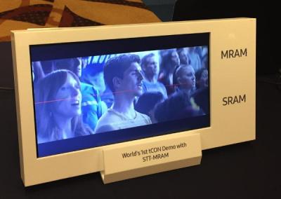
Samsung demonstrated an LCD display that uses a tCON chip that uses embedded 28nm pMTJ STT-MRAM memory, instead of the normally used SRAM. The MRAM device had a density of 8Mb and a 1T-1MTJ cell architecture. The cell size is 0.0364 um2.

Samsung LCD tCON Demo (IEDM-2017)

A tCON chip is a timing controller chip that processes the video signal input and processes it to generate control signal to the source & gate driver of the LCD display. The memory is used a a frame memory which stores previous frame data. Samsung prepared a test chip that contains both SRAM and MRAM memory devices to show that there is no difference between the two. SRAM replacement is a popular MRAM application.

Read the full story Posted: Dec 12,2016

Global Foundries to offer Everspin's PMTJ STT-MRAM as an embedded memory solution

Everspin announced that its perpendicular (pMTJ) STT-MRAM memory is going to be deployed by Global Foundries as an embedded 22nm memory. Everspin licensed its technology global foundries which will offer this as part of its 22FDX platform.

Global Foundries 22nm eMRAM slide

The 22FDX platform targets emerging applications such as battery powered consumer devices, IoT, Advanced Driver Assistance Systems (ADAS) and Vision Processing. Customers of Global Foundries will now be able to embed MRAM memory in next-generation SoC and MCU based producers.

Read the full story Posted: Sep 16,2016

Avalanche Technology announce four additional key MRAM and STT-MRAM patents

Avalanche Technology has been awarded new key patents in the areas of STT-MRAM technology, MRAM integration and manufacturing and perpendicular Magnetic Tunnel Junction (pMTJ) STT-MRAM. This follows eight new key patents awarded to Avalanche since the beginning of 2014.

Avalanche (founded in 2006 and based in California, US) developed patented Spin Programmable STT-MRAM (SPMEM) memory that uses a revolutionary proprietary spin current and voltage switching technology. The company wants to license their technology for embedded applications and also build discrete standalone memory devices. In July 2012 the company raised $30 million.

Read the full story Posted: Aug 08,2014

Imec to collaborate with Canon Anelva on STT-MRAM R&D

Belgian's research center Imec announced today that it will collaborate with Canon Anelva on STT-MRAM research and development. This collaboration will be part of imec's R&D program on advanced emerging memory technologies and aims to explore the full technology potential of STT-MRAM including performance beyond 1ns and scalability beyond 10 nm for embedded & stand alone applications.

Canon Anelva already installed a deposition tool in imec’s state-of-the-art 300-mm clean room. Combined with imec’s advanced litho-cluster and its material engineering capabilities, imec’s industrial partners now have access to a complete 300-mm STT-MRAM-dedicated processing capability.

Read the full story Posted: Nov 12,2012

Need for Smaller, High-speed, Ultra-high Density, Storage Devices Fostering Advances in Embedded Memories

Research and Markets has announced the addition of the Frost & Sullivan report: Advances in Embedded Memories to their offering.

In this research, Frost & Sullivan's expert analysts thoroughly examine the following technologies: embedded static random access memory (eSRAM), embedded dynamic RAM (eDRAM), embedded flash memory (eflash), magnetoresistive RAM (MRAM), ferroelectric RAM (FeRAM/FRAM), phase change memory (PCM/PRAM), carbon nanotube memory, molecular memory, polymer memory, and biomolecular memory.

Read the full story Posted: May 30,2007

NEC Develops MRAM Cell Technology Suitable for Embedding in Next Generation System LSIs

NEC Corporation today announced that it has succeeded in developing new MRAM cell technology suitable for high speed memory macro embedded in next generation system LSIs. The newly developed cell technology includes three key elements; a 2T1MTJ (two transistors and one magnetoresistive tunneling junction) cell structure to accelerate write mode cycle time, a 5T2MTJ cell structure to accelerate read mode cycle time and a write-line-inserted MTJ to reduce write current. The new cell technology realizes added-value, non-volatile MRAM macros that can be substituted for SRAM (static random access memory) macros embedded in system LSIs.

Features of the newly developed elements:
1. 200MHz random access write operation: Elimination of the upper limit of the writing current by a 2T1MTJ cell enables high speed write operation. In conventional MRAM memory cells, writing current must be within upper and lower limits (note 1). This complicates the write current source circuit and it thus cannot operate at over 100MHz.
2. 500MHz random access read operation: Intra-cell-signal amplification in a 5T2MTJ cell enables high speed read operation. Cell current signal is amplified and transformed into voltage signal in each cell. In conventional MRAM memory cells, a small reading current difference signal through the bit line with large parasitic capacitance makes sense amplifier circuits complicated. These kinds of circuits cannot operate at over 200MHz.
3. Reduction of writing current down to 1/3: A write-line-inserted MTJ structure reduces writing current to 1/3 as compared with conventional MTJ structure writing currents. This small current reduces MRAM cell size.

Read the full story Posted: Jul 14,2006

Embedded non-volatile storage promises memory marvels

Interesting article from Engineer Live, about MRAM, OUM and FRAM -
MRAM is the highest profile at the moment, with a 4Mbit prototype shown in December (2003) based around a magnetic tunnel junction (MTJ) where magnetic material stores the data bit.
"We are very excited about this," said Saied Tehrani, director of MPEM technology at Motorola Semiconductor division. "It really brings two parts of the industry together - semiconductor and magnetics. We have taken the thin film technology and integrated that with the silicon transistor technology and used the magnetic polarisation to store the data and the silicon transistor for reading and writing the information."
The 4Mbit part is built in 0.18µm technology but for commercial products Motorola is looking at jumping a process generation and going straight to the current leading edge 90nm. This is being developed at a plant in Crolles, France, in a joint development with Franco-Italian chip maker ST Microelectronics and Dutch electronics giant Philips.
This would allow 64Mbits or even 128Mbit stand alone devices to be built, but that is not the aim.
So Motorola is planning to embed MRAM into devices alongside other functions. Tehrani would not comment on what these devices would be, except to say that they would be out on the market in 2005 and Motorola would announce the roadmap later this year. "Microcontrollers are a definite possibility for this technology," he said.

Read the full story Posted: Jun 04,2005