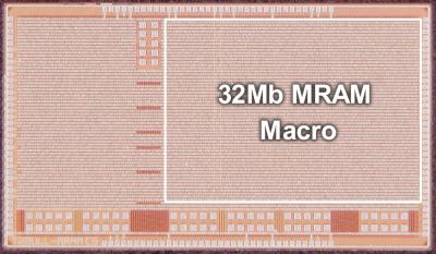
Renesas announced that it has developed 22-nm embedded STT-MRAM circuit technologies. Renesas developed a test 32-megabit (Mbit) chip with an embedded MRAM memory cell array that achieves 5.9-nanosecond (ns) random read access at a maximum junction temperature of 150°C, and a write throughput of 5.8-megabyte-per-second (MB/s).
To achieve this performance, Renesas developed two technologies. The first is a fast read technology employing high-precision sense amplifier circuit, utilizing capacitive coupling. The second is a fast write technology, with simultaneous write bit number optimization and shortened mode transition time.
The write technology divides up the areas to which write voltage is applied and, by inputting the write address before the write voltage setup, it selectively applies voltage only to the necessary area. This method reduces the parasitic capacitive load on the area where the voltage is applied during the write operation, reducing the voltage setup time. As a result, the mode transition time to write operation is reduced by approximately 30%, speeding up write operation.
Renesas says it continues to develop technologies aimed at the application of embedded MRAM technology in MCU products. These new technologies have the potential to dramatically boost memory access speed, which is currently a challenge with MRAM, to exceed 100 MHz, enabling higher-performance MCUs with embedded MRAM. Faster write speed will contribute to more efficient code writing to endpoint devices. Renesas is committed to further increasing capacity, speed, and power efficiency for MCUs to accommodate a range of new applications.