STT-MRAM (also called STT-RAM or sometimes ST-MRAM and ST-RAM) is an advanced type of MRAM devices. STT-MRAM enables higher densities, low power consumption and reduced cost compared to regular (so-called Toggle MRAM) devices. The main advantage of STT-MRAM over Toggle MRAM is the ability to scale the STT-MRAM chips to achieve higher densities at a lower cost.

STT-MRAM has the potential to become a leading storage technology as it is a high-performance memory (can challenge DRAM and SRAM) that can scale well below 10nm and challenge the low cost of flash memory.

What is STT-MRAM?

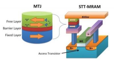
STT stands for Spin-Transfer Torque. In an STT-MRAM device, the spin of the electrons is flipped using a spin-polarized current. This effect is achieved in a magnetic tunnel junction (MTJ) or a spin-valve, and STT-MRAM devices use STT tunnel junctions (STT-MTJ). A spin-polarized current is created by passing a current though a thin magnetic layer. This current is then directed into a thinner magnetic layer which transfers the angular momentum to the thin layer which changes its spin.

What is perpendicular STT-MRAM?

A "regular" STT-MRAM structure (similar to the one you see above) uses an in-plane MTJ (iMTJ). Some STT-MRAM devices use a more optimized structure called perpendicular MTJ (pMTJ) in which the magnetic moments are perpendicular to the silicon substrate surface.

Perpendicular STT-MRAM is more scalable compared to iMTJ STT-MRAM and is also more cost competitive. Perpendicular STT-MRAM is thus a more promising technology to replace DRAM and other memory technologies

STT-MRAM chips

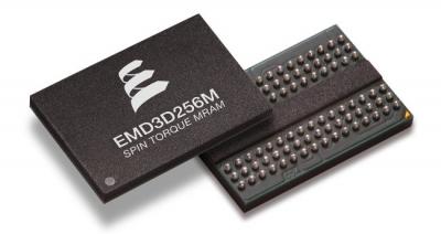
Several companies, including IBM and Samsung, Everspin, Avalanche Technologies, Spin Transfer Technologies and Crocus are developing STT-MRAM chips. In April 2016 Everspin announced that it started shipping 256Mb ST-MRAM samples to customers. The new chips demonstrate interface speeds comparable to DRAM, with DDR3 and DDR4 interfaces. Volume production is expected "soon".

In August 2016 Everspin started sampling pMTJ-based ST-MRAM chips. The first chips are also 256Mb in size, but the pMTJ versions offer improved performance, higher endurance, lower power, and better scalability compared to previous iMTJ ST-MRAM products. Everspin is now ramping out 256Mb pMTJ ST-MRAM production and is developing a scaled-down 1Gb version.


Latest STT-MRAM news

GlobalFoundries and Everspin say that the pMTJ STT-eMRAM features high reliability at high temperatures

GlobalFoundries has plans to deploy Everspin's perpendicular (pMTJ) STT-MRAM as an embedded 22nm memory - as part of GF's 22FDX platform. GlobalFoundries has released a technical paper that details the eMRAM ability to retain data at high temperatures.

Global Foundries 22nm eMRAM slide

The eMRAM can retain data through solder reflow at 260 degrees Celsius, and for more than 10 years at 125 degrees Celsius, plus read/write with outstanding endurance at 125 degrees Celsius. GlobalFoundries says that this will enable eMRAM to be used for general purpose MCUs and automotive SOCs.

Read the full story Posted: Jun 30,2017

Samsung reaffirms 2018 target for STT-MRAM mass production

During Samsung Electronic's Foundry Forum, the Korean chip maker reaffirmed its goal to start producing STT-MRAM chips in 2018. In fact Samsung now says that it will mass produce these chips next year, while last year it said that 2018 will only see limited production while real mass production will only begin in 2019.

Samsung announced it will produce the 2018 MRAM chips will be produced using 8-nano low power plus (8LMPP) semiconductor foundry process. Samsung sees MRAM produced by 4LPP by 2020.

Read the full story Posted: May 26,2017

Everspin announces new MRAM customers and products

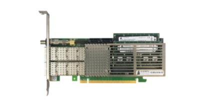
Everspin announced several new applications and customers for its MRAM solutions. First up is the new nvNITRO storage accelerator product family. These new cards (aimed for demanding applications such as financial transactions) are available in either 1Gb or 2Gb, and are based on Everspin's 256Mb DDR STT-MRAM chips. Later this year Everspin will release new models based on its 1Gb DDR4 chips which will enable capacities up to 16Gb.

Everspin nvNITRO NVMe PCIe STT-MRAM card photo

Everspin says that the nvNITRO operate at a very fast 1,500,000 IOPS with 6-ms end-to-end latency. Everspin is testing the first cards at customers now, and initial production will begin in Q2 2017.

Read the full story Posted: Mar 10,2017

Toshiba and Hynix prototype a 4 Gb STT-MRAM

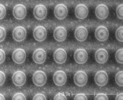
Toshiba and SK Hynix co-developed a 4-Gbit STT-MRAM chip, and presented a prototype at IEDM 2016.

Toshiba Hynix 4Gb STT-MRAM mTJ array photo

The prototype chip is made from eight 512-Mbit banks, and the cell area is equivalent to that of DRAM - at 9F2, which Hynix says is much smaller than conventional STT-MRAMs (50F2).

Read the full story Posted: Dec 20,2016

Samsung demonstrates a 8Mb embedded pMTJ STT-MRAM device

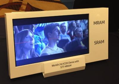
Samsung demonstrated an LCD display that uses a tCON chip that uses embedded 28nm pMTJ STT-MRAM memory, instead of the normally used SRAM. The MRAM device had a density of 8Mb and a 1T-1MTJ cell architecture. The cell size is 0.0364 um2.

Samsung LCD tCON Demo (IEDM-2017)

A tCON chip is a timing controller chip that processes the video signal input and processes it to generate control signal to the source & gate driver of the LCD display. The memory is used a a frame memory which stores previous frame data. Samsung prepared a test chip that contains both SRAM and MRAM memory devices to show that there is no difference between the two. SRAM replacement is a popular MRAM application.

Read the full story Posted: Dec 12,2016

IMEC researchers demonstrate the world's smallest pMTJ at 8nm

Researchers at IMEC developed a 8nm perpendicular magnetic tunnel junction (pMTJ) with 100% tunnel magnetoresistance (TMR) and a magnetic coercive field up to 1,500 Oe in strength. The researchers also demonstrated integrated 1Mbit STT-MRAM 1T1MTJ arrays with pitches down to 100 nm.

IMEC says that this is the world's smallest pMTJ - which paves the way for high density stand-alone MRAM applications. The pMTJ was developed on 300mm silicon wafers in a production process that is compatible with the thermal budget of standard CMOS back-end-of-line technology.

Read the full story Posted: Dec 07,2016

The EU-funded GREAT project presents its first hybrid CMOS-MRAM 180nm tape out

GREAT Project logoIn 2015, the EU launched the GREAT project, with an aim to co-integrate multiple functions like sensors, RF receivers and logic/memory together within CMOS by adapting STT-MTJs to a single baseline technology in the same system on chip. GREAT stands for heteroGeneous integRated magnetic tEchnology using multifonctionnal stAndardized sTack.

The project partners now announced the first hybrid CMOS/MSS-MRAM Tape Out with Israel-based Tower Jazz. This hybrid integrated circuit uses the 180nm CMOS process from Tower and an academic MRAM post-process that will be done by CEA Spintec within their facilities.

Read the full story Posted: Nov 20,2016

Interview with Bo Hansen, CEO at Capres A/S

Bo Hansen, Capres CEOCapres A/S was established in 1999 in Denmark to develop a unique probe technology designed for in-line production monitoring in the semiconductor industry. The company, in collaboration with IBM, developed a resistivity measurement technique to characterize MTJ stacks.

Bo Svarrer Hansen, the company's CEO since 2002, was kind enough to answers a few questions we had, and share with us his views on the MRAM market and the company's measurement systems for MRAM and STT-MRAM device developers.

Q: Can you update us on Capres' current offers to the MRAM industry?

Capres customers are using our CIPTech® tools for R&D on small samples as well as volume production on 300 mm wafers. Depending on the configuration the tools measure with an in- plane or an out- of- plane magnetic field on blanket as well as patterned wafers.

Read the full story Posted: Oct 26,2016