 Capres A/S was established in 1999 in Denmark to develop a unique probe technology designed for in-line production monitoring in the semiconductor industry. The company, in collaboration with IBM, developed a resistivity measurement technique to characterize MTJ stacks.
Bo Svarrer Hansen, the company's CEO since 2002, was kind enough to answers a few questions we had, and share with us his views on the MRAM market and the company's measurement systems for MRAM and STT-MRAM device developers.
Q: Can you update us on Capres' current offers to the MRAM industry?
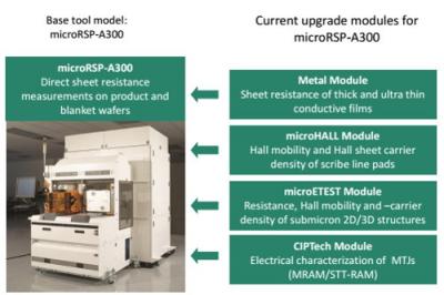
Capres customers are using our CIPTech® tools for R&D on small samples as well as volume production on 300 mm wafers. Depending on the configuration the tools measure with an in- plane or an out- of- plane magnetic field on blanket as well as patterned wafers.
Q: Can you explain the measurement technique co-developed with IBM?
Daniel Worledge from IBM got the idea for The Current In Plane Tunneling-, or "CIPT", measurement technique back in 2001 and realized that a four point probe with a few micrometer pitch was needed in order to do the measurements. He teamed up with CAPRES, a young company then, and based on Daniels ideas CAPRES developed the first microscopic 12 point CIPTech® probe and the first CIPTech® tool.
A magnetic tunnel junction is characterized by measuring the sheet resistance with various pitches on the same location for both the high and the low state of the magnetic tunnel junction. This information is fed through a mathematical model that calculates the RA and the MR values, the two most important parameters for an MTJ. Since the CIPTech® measurements are made directly on the sample without any preparations they only take seconds compared to the alternative, which is a short loop that takes days.
Q: Do you still collaborate with IBM on MRAM research?
We cannot reveal our current collaboration partners, but IBM is certainly one of the leading companies in the MRAM industry
Q: Is there a difference between MRAM and STT-MRAM measurement techniques?
The same algorithm, developed by IBM, which is used for both MRAM and STT-MRAM measurements.
Q: In 2009 it was reported that Crocus acquired a CAPRES measurement system. Do you still work with Crocus? Can you share any other MRAM customers besides Crocus?
Since we delivered the first CIPTech® to IBM in 2003 we have sold our systems to all the major players in the semiconductor industry. Last year we delivered a fully automated CIPTech ® tool to a high volume 300mm fab.

Q: I've been following MRAM for over 10 years, and in past months it seems like the MRAM market is finally getting some traction (besides Everspin's excellent MRAM work, of course). Do you share this feeling?
Based on our dialogue with our customers we have seen a steady increase in their activity level and we expect that other companies besides GlobalFoundries will be manufacturing MRAM in their 300 mm fabs within 1-2 years. As an example we can see the newly announced Avalanche-Sony partnership for manufacturing of Avalanche STT-MRAM by Sony in 2017.
Q: STT-MRAM is slowly entering the market, where do you see this technology being adopted in the next 3-5 years?
We see STT-MRAM entering the market within 1-2 years as embedded memory on high performance logic chips. Standalone STT-MRAM will come later and the adaption rate will depend strongly on the price.
Q: Do you think MRAM has a chance to become a real game changer in the storage industry? Or will it remain a high-end niche technology?
I believe that STT-MRAM will replace SRAM and has a good chance to replace DRAM if it becomes cost efficient enough.

