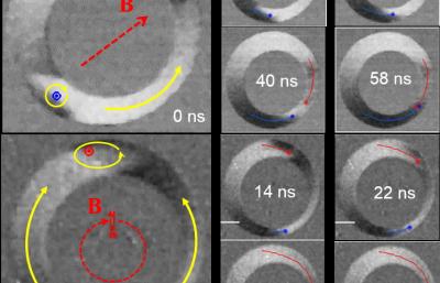
Multi-layered Co/Ni films are highly desirable materials for effective spin transfer torque

Researchers from the University of Lorraine in France have discovered that multilayers films made of cobalt (Co) and nickel (Ni) hold great promise for STT-MRAM applications.
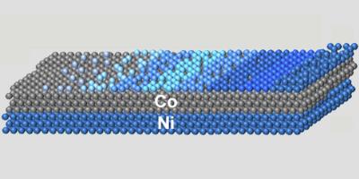
Multi layered cobalt and nickel films for spintronics

It was already shown before that Co/Ni multilayers have very good properties for spintronics applications, but up until now it wasn't clear if the films have a sufficiently large intrinsic spin polarization, which is necessary to create and maintain spin-polarized currents in spintronic devices. It was now shown that the films have a spin polarization of about 90% - which is similar to the best spintronic materials.
Read the full story Posted: Jun 30,2018

Imec researchers deposited SOT-MRAM devices on 300 mm wafers

Researchers from Imec fabricated spin-orbit torque MRAM (SOT-MRAM) devices on 300mm wafers using CMOS compatible processes. The researchers say that these devices offer unlimited endurance, fast switching speeds and low power consumption.

Imec says that SOT-MRAM can overcome the limitation of spin-transfer torque in MRAM memories, but up until now it was only demonstrated in a lab. The core of the SOT-MRAM is a magnetic tunnel junction in which a thin dielectric layer is sandwiched between a magnetic fixed layer and a magnetic free layer. SOT-MRAM devices feature switching of the free magnetic layer done by injecting an in-plane current in an adjacent SOT layer, unlike STT-MRAM where the current is injected perpendicularly into the magnetic tunnel junction and the read and write operation is performed through the same path.

Read the full story Posted: Jun 19,2018

Researchers develop a process to form single-crystal CMRs on metal wires

Researchers from Japan's National Institute of Advanced Industrial Science and Technology (AIST) developed a new process, based on 3D stacking, that forms a single-crystal TMR device on a polycrystal metal wire.

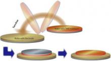
3D TMR-MRAM stacking process (AIST)

The stacking process creates the TMR thin-film on a single-crystal silicon wafer and then bonds it to a CMOS on another wafer. This opens the way to using these materials in high-performance MRAM devices. The single-crystal TMRs reduces the variation in the device and can enable smaller TMRs. The researcher say that it will take up to 2 years to completely develop the new 3D stacking process.

Read the full story Posted: May 14,2018

The EU GREAT Project delivered its 2nd tape-out demonstrator

In 2015, the EU launched the GREAT project, with an aim to co-integrate multiple functions like sensors, RF receivers and logic/memory together within CMOS by adapting STT-MTJs to a single baseline technology in the same system on chip. GREAT stands for heteroGeneous integRated magnetic tEchnology using multifonctionnal stAndardized sTack.

GREAT Project 2nd tape-out photo

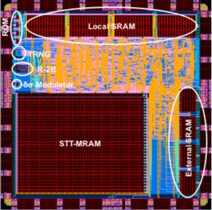
After the delivery of a first demonstrator in 2017, the project partners now announced the second hybrid CMOS/MSS-MRAM 180nm Tape Out at Israel-based Tower Jazz. The project partners designed four ICs to validate Analog IP blocks and an ultra-low power MCU comprising a hardware security block.

Read the full story Posted: May 04,2018

Spin Transfer Technologies announces a breakthrough new STT-MRAM technology

Spin Transfer Technologies (STT) announced that its unique Precessional Spin Current (PSC) structure can increase the spin-torque efficiency of any MRAM device by 40-70 percent, which means dramatically higher data retention while consuming less power.

Following advanced testing, the company says that these higher spin-torque efficiencies translate to retention times lengthening by a factor of over 10,000 while reducing write current.

Read the full story Posted: Apr 30,2018

Tohoku University develops ultra-small (<10nm) MTJs

Researchers from Tohoku University developed new ultra-small (single-digit nanometer scale) magnetic tunnel junctions (MTJs) that have sufficient retention properties and yet can be switched by a current.

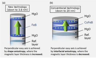
Shape anisotropy and interfacial anisotropy MTJs (Tohoku University)

Tohoku University developed 20-nm CoFeB/MgO-based MTJs in 2010, in which an "interfacial anisotropy" at the CoFeB/MgO interface was utilized. But these will not work at under 20-nm. The researchers now used a "shape anisotropy" to achieve the smaller MTJs.

Read the full story Posted: Feb 22,2018

Keysight Technology announces a new MRAM test platform designed in collaboration with Tohoku University

Tohoku University's Center for Innovative Integrated Electronic System (CIES) announced that its collaboration with Keysight Technology has led to the release of a new MRAM test platform product, the NX5730A.

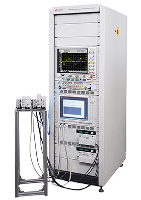
Kesight NX5730A Memory Test system photo

Keysight's NX5730A is a high-throughput 1 ns Pulsed IV memory test solution. Keysight says that this solution is a unique dedicated system for characterizing emerging devices such as magnetic tunnel junction (MTJ) on silicon wafers, accelerating the efficiency of device characterization and memory production testing.

Read the full story Posted: Nov 08,2017

A new method to control magnetism could lead to ultra-fast and more efficient MRAM chips

Researchers from UC Berkeley and UC Riverside developed a new ultra-fast method for electrically controlling magnetism in certain metals. The researchers say that this could be applied to future MRAM chips, to provide much faster write speeds and more efficient operation.

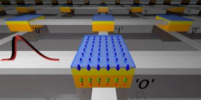
Ultrafast electrical magnetic switching (UCB + UCR)

The researchers built special circuits to study how magnetic metals respond to electrical pulses as short as a few picoseconds. The researchers found that in a magnetic alloy made up of gadolinium and iron, these fast electrical pulses can switch the direction of the magnetism in less than 10 picoseconds, orders of magnitude faster than any other MRAM technology.

Read the full story Posted: Nov 04,2017

A new European project aims to develop a system-level STT-MRAM exploration flow

The EU launched a new project called GREAT H2020 moderated by the CEA-Spintec laboratory that plans to co-integrate multiple functions like sensors, RF receivers and logic/memory together within CMOS thanks to a single baseline technology in the same System on Chip.

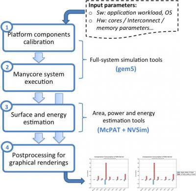
MAGPIE process image

One of the project’s final objectives is to develop a system-level simulation and design of a representative IoT platform, integrating this technology. To achieve it, a unique exploration flow is proposed: MAGPIE. MAGPIE stands for Manycore Architecture enerGy and Performance evaluation Environment and has been jointly developed and funded through GREAT and the CONTINUUM ANR French project.

Read the full story Posted: Oct 12,2017