Samsung demonstrates a 8Mb embedded pMTJ STT-MRAM device

Samsung demonstrated an LCD display that uses a tCON chip that uses embedded 28nm pMTJ STT-MRAM memory, instead of the normally used SRAM. The MRAM device had a density of 8Mb and a 1T-1MTJ cell architecture. The cell size is 0.0364 um2.

Samsung LCD tCON Demo (IEDM-2017)

A tCON chip is a timing controller chip that processes the video signal input and processes it to generate control signal to the source & gate driver of the LCD display. The memory is used a a frame memory which stores previous frame data. Samsung prepared a test chip that contains both SRAM and MRAM memory devices to show that there is no difference between the two. SRAM replacement is a popular MRAM application.

Read the full story Posted: Dec 12,2016

IMEC researchers demonstrate the world's smallest pMTJ at 8nm

Researchers at IMEC developed a 8nm perpendicular magnetic tunnel junction (pMTJ) with 100% tunnel magnetoresistance (TMR) and a magnetic coercive field up to 1,500 Oe in strength. The researchers also demonstrated integrated 1Mbit STT-MRAM 1T1MTJ arrays with pitches down to 100 nm.

IMEC says that this is the world's smallest pMTJ - which paves the way for high density stand-alone MRAM applications. The pMTJ was developed on 300mm silicon wafers in a production process that is compatible with the thermal budget of standard CMOS back-end-of-line technology.

Read the full story Posted: Dec 07,2016

The EU-funded GREAT project presents its first hybrid CMOS-MRAM 180nm tape out

GREAT Project logoIn 2015, the EU launched the GREAT project, with an aim to co-integrate multiple functions like sensors, RF receivers and logic/memory together within CMOS by adapting STT-MTJs to a single baseline technology in the same system on chip. GREAT stands for heteroGeneous integRated magnetic tEchnology using multifonctionnal stAndardized sTack.

The project partners now announced the first hybrid CMOS/MSS-MRAM Tape Out with Israel-based Tower Jazz. This hybrid integrated circuit uses the 180nm CMOS process from Tower and an academic MRAM post-process that will be done by CEA Spintec within their facilities.

Read the full story Posted: Nov 20,2016

Researchers developed a spin-orbit torque based device, an alternative to STT

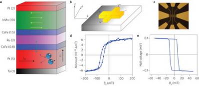
Researchers from the Trinity College in Dublin developed a new device using a stack of five metal layers (including a platinum layer and an iron-based layer) that can be used to control the spin of electrons - using "spin–orbit torque", or SOT, an alternative to spin-transfer torque (STT) - but without an external field.

SOT switching without an eternal field (TCD)

The basic idea is that when a current is run through the platinum, the electrons split into two groups by their spin (that's the SOT effect). Electrons are inserted into the iron-based "storage layer" and the spin of those electrons can be changed. The rest of the layers act like a thin-film magnet which helps determine the spin of the electrons.

Read the full story Posted: Jul 22,2016

NUS researchers developed the world's first bendable MRAM device

Researchers from the National University of Singapore (NUS) developed what they say is the world's first flexible (bendable, actually) MRAM device. Flexible OLED displays are already entering the market, and now researchers are developing other flexible components, which will be needed if truly bendable and flexible devices are to be possible.

Flexible MRAM device, NUS 2016

The researchers used a new fabrication method, that enabled them to deposit the magnetic memory on a plastic substrate, and not a silicon one. This was achieved following a two-year collaboration with Yonsei University, Ghent University and Singapore's Institute of Materials Research and Engineering.

Read the full story Posted: Jul 20,2016

IBM demonstrated 11nm STT-MRAM junction, says "time for STT-MRAM is now"

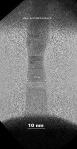
IBM researchers, in collaboration with Samsung researchers, demonstrated switching MRAM cells for devices with diameters ranging from 50 down to 11 nanometers in only 10 nanoseconds, using only 7.5 microamperes. The researchers say that this is a significant achievement on the way to high-density low-power STT-MRAM.

IBM TEM image of a 11-nm junction

Using perpendicular magnetic anisotropy (PMA), the researchers can deliver good STT-MRAM performance down to 7×10⁻¹⁰ write-error-rate with 10 nanosecond pulses using switching currents of only 7.5 microampere.

Read the full story Posted: Jul 08,2016

Israeli researchers develop six-state magnetic memory elements

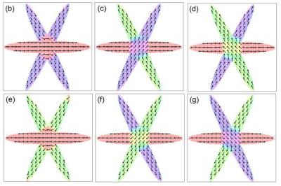
Researchers from Israel's Bar Ilan University and New York University designed a six-state magnetic element - which could be used to create a magnetic memory device with six-states - and thus a higher density than a the regular 2-state device.

Simulated six-state magneic memory

The researchers say that multi-level MRAM cells based on this design should not suffer from low writing speed and high power consumption - problems that are common in multi-level Flash memory cells.

Read the full story Posted: May 19,2016

Researchers develop a way to increase STT-MRAM density by placing MTJs directly on the via

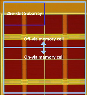
Researchers from Japan's Tohoku University developed a technology to stack magnetic tunnel junctions (MTJs) directly on the the vertical interconnect access (via) without causing deterioration to its electric/magnetic characteristics. The researchers say that this technique can reduce the chip area of STT-MRAM.

Tohoku on-via STT-MRAM cell

The via in an integrated circuit design is a small opening that allows a conductive connection between the different layers of a semiconductor device. Placing the MTJ directly on the via holes has been avoided because it can degrade the MTJ's characteristics because the MTJ is very sensitive to the quality of the surface of its lower electrode.

Read the full story Posted: May 17,2016

Researchers suggest and demonstrate a new scheme of spin-orbit-torque (SOT) induced magnetization switching

Researchers at Tohoku University developed a new scheme of spin-orbit-torque (SOT) induced magnetization switching. In the new scheme the magnetization directed collinear with the current.

Structures of spin orbit torque induced magnetization


The researcher fabricated three-terminal devices with the new structure (using a Ta/CoFeB/MgO-based magnetic tunnel junction) and successfully demonstrated the switching operation. The research report a "reasonably small" required current density to induce the magnetization switching and a "reasonably large" resistance difference between 0 and 1 states. They say that this is a promising candidate for future MRAM devices.

Read the full story Posted: Mar 22,2016