Hynix to produce PRAM memory by 2009

Hynix aims to produce a next-generation memory chip called Phase-change Random Access Memory (PRAM) by 2009. Industry analysts expect it to become the main memory device, replacing high-density flash memories, within the next decade.

Read the full story Posted: Jul 26,2007

Need for Smaller, High-speed, Ultra-high Density, Storage Devices Fostering Advances in Embedded Memories

Research and Markets has announced the addition of the Frost & Sullivan report: Advances in Embedded Memories to their offering.

In this research, Frost & Sullivan's expert analysts thoroughly examine the following technologies: embedded static random access memory (eSRAM), embedded dynamic RAM (eDRAM), embedded flash memory (eflash), magnetoresistive RAM (MRAM), ferroelectric RAM (FeRAM/FRAM), phase change memory (PCM/PRAM), carbon nanotube memory, molecular memory, polymer memory, and biomolecular memory.

Read the full story Posted: May 30,2007

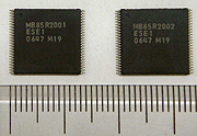
2Mbit FRAM chips for high-speed data writing from Fujitsu

Fujitsu's MB85R2001 and MB85R2002 feature non-volatile memory with high-speed data writing, low power consumption and the ability to provide a large number of write cycles.

The MB85R2001 and MB85R2002 FRAM chips are ideal for automotive navigation systems, multifunction printers, measuring instruments and other advanced applications that can use non-volatile memory to store various parameters, record equipment operating conditions and preserve security information.

The configuration of MB85R2001 is 256K words x 8bits, while the configuration of MB85R2002 is 128K words x 16 bits. Both MB85R2001 and MB85R2002 feature read access times of 100ns and read/write cycle times of 150ns. The MB85R2001 and MB85R2002 operate from 3V to 3.6V.

Read the full story Posted: May 29,2007

Intel Says PRAM Volume Production to Start in 2H of 2007

Intel Corp. has revealed a prototype PRAM (phase change RAM) wafer, long under development, at IDF Spring 2007 in Beijing, China, which began on April 16, 2007. At the keynote speech, Intel's CTO Justin Rattner announced, "the company will start mass-production of PRAM as early as the second half of 2007." He also said, "We consider replacing NOR flash memory with PRAM first, but that's not our goal. PRAM may possibly replace DRAM in the near future. We are paying a lot of attention to the technology."

Read more here (TechOn) 

Read the full story Posted: Apr 19,2007

Fujitsu Starts Volume Production of 2 Mbit FRAM Chips

Fujitsu today announced the availability of its 2 Mbit Ferroelectric RAM (FRAM or FeRAM) memory chips, which the company claims is the largest capacity FRAM in volume production in the world. The memory product have the same electrical characteristics and use the same TSOP-48 package as Fujitsu's 1 Mbit FRAM products, equating to double the capacity over previous chips.

Sampling price of the chips is set at 2,000 Yen ($16.91 USD).

Read the full story Posted: Apr 19,2007

Intel set for first public demo of PRAM

PRAM is based on chalcogenide glass, which can be altered using the heat generated by an electric current. Heat changes the physical structure of the glass to either a crystalline or amorphous state. Each of these states has a distinct electrical resistance that is used to represent the ones and zeroes needed to represent stored data in binary terms.

Read the full story Posted: Apr 17,2007

Intel to sample PRAM this year

Intel's new phase-change memory technology, called PRAM by Intel and PCM by others who are working on the same type of memory, is set to sample in the first half of this year. Intel says they plan to ship the first PRAM modules as a straight-ahead NOR flash replacement so that they can work the kinks out of the design before trying to move it up the memory hierarchy. The company claims a much higher number of read-write cycles (100 million) than flash, as well as a potential 10 years' worth of data retention.

Read more here (ars technica)

Read the full story Posted: Mar 11,2007

Hitachi and Renesas develop phase-change memory

In addressing the need for next-generation high-density on-chip non-volatile memory Technology, Hitachi, Ltd. and Renesas today announced the development of a 512-kbyte (4-Mbit equivalent) phase change memory module operating at a 1.5-V power supply voltage, which achieves 416-kbyte/sec high-speed write and read speeds with a 20-nanosecond access time. Using the previously developed "low-power phase change memory cells" with a 100-uA (micro(2)-ampere) write current, the two companies developed a peripheral circuit Technology to enable the high-speed write and read operations.

An experimental 512-kbyte memory module was fabricated using a 130-nm CMOS process, employing the newly developed circuit Technology for cells writable at 100 uA. Test results confirmed the possibility of 416-kbyte/sec write operations and 20-nanosecond read operations, and high-speed operation was achieved while maintaining the Performance of low-power-operation phase change memory cells.

Read the full story Posted: Feb 20,2007

Hitachi, Tohoku Univ. Jointly Prototype 2 Mbit Nonvolatile RAM Based on Spin Torque Transfer

Hitachi, Ltd. and Prof. Hideo Ohno of The Research Institute of Electrical Communication, Tohoku University have jointly prototyped a 2 Mbit nonvolatile RAM chip based on the spin torque transfer writing technology. When a 1.8 V voltage is supplied, the write and read times are 100 and 40 ns, respectively. TMR elements used in the chip were produced by the Tohoku Univ. lab while the chip designed with a 0.2 ?m rule process technology was manufactured by Hitachi. The details were presented at the ISSCC 2007 event being held in San Francisco on February 14 (US time).

Write current of 200 mA, cell size of 16F2

The nonvolatile RAM based on spin torque transfer is designed to eliminate write lines for magnetic field generation used in a magnetoresistive RAM (MRAM). Instead, data rewriting is performed by the current flown through memory elements (TMR elements). In this way, the spin torque transfer RAM can solve a problem of the write current in MRAM which increases as miniaturization accelerates. Thus far, Hitachi and Tohoku Univ. have jointly examined the principles of this method at the element level.

The write current of the prototyped RAM is 200 ?A/cell, lower than that of a standard MRAM. It was demonstrated that data can be rewritten 109 times with a 100 ns pulse current. The chip measures 5.32 x 2.5 mm. The cell size is 1.6 x 1.6 ?m, which is equivalent to 16F2 (F is the design rule of cell section which equals to 0.4 ?m). This is smaller than a standard MRAM cell. It is reported that 10F2 is also feasible by improving the design layout. The magnetoresistance ratio of the TMR element is approximately 100. Incidentally, Sony Corp. presented a prototype of 4 Kbit Nonvolatile RAM based on spin torque transfer at the 2005 IEDM event. The capacity of the latest MRAM is nearly three orders of magnitude larger than that of Sony's product.

Read more here (TechOn)

Read the full story Posted: Feb 15,2007

Ovonyx reports a new license for OUM memory

ECD Ovonics' Ovonyx, Inc. joint venture secured a new license with Qimonda AG to commercialize Ovonic Unified Memory (OUM) technology.

Additionally, a joint research program consisting of Qimonda, IBM and Macronix announced positive research results for a prototype phase-change memory device that they had designed, built and demonstrated.
Read the full story Posted: Feb 09,2007