SOT-MRAM - Page 2

NTU and TSMC researchers develop a new SOT-MRAM structure with high spin-orbital Hall conductivity

Researchers from National Taiwan University in collaboration with TSMC developed a new SOT-MRAM device structure, that features sizable orbital currents. This research promises a pathway for enhancing SOT-MRAM performance by harnessing both the conventional spin currents and the emergent orbital currents.

NTU TSMC PtCr Alloys SOT-MRAM
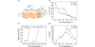
The new device is based on 3d light transition metals (such as V and Cr) that are incorporated into the classical spin Hall metal Pt. The Pt-Cr alloy enhances the charge-to-spin conversion efficiency which can realize high spin-orbital Hall conductivity, beyond the conventional spin Hall limit.

Read the full story Posted: Feb 27,2022

Researchers developed an ultra low power BiSb-based SOT MRAM device

Researchers from the Tokyo Institute of Technology developed an ultrahigh-efficiency SOT magnetization switching in fully sputtered BiSb(Co/Pt) multilayers with large perpendicular magnetic anisotropy (PMA).

Scheme of ultra low power BiSb SOT-MRAM device (Tokyo IT)

The new device offers a large spin Hall angle and high electrical conductivity, thus satisfying all the three requirements for SOT-MRAM implementation. The researchers managed to achieve robust SOT magnetization at a low current density despite the large PMA field.

Read the full story Posted: Feb 23,2022

Hprobe launches a next-generation MRAM wafer sort magnetic test head

Hprobe announced a new magnetic test head for MRAM Wafer Sort. The new module, the H3DM-XL, is at the heart of the latest addition to Hprobe’s IBEX line, the IBEX-WS.

Hprobe MRAM Wafer-Sort Magnetic Test Head (IBEX-WS)

The IBEX-WS test equipment integrates 3D magnetic field capabilities, while increasing field area and uniformity for wafer probing large MRAM arrays. It also features a unique patented robotized 3D Field Calibration Unit (FCU) for high-speed field mapping and monitoring.

Read the full story Posted: Dec 01,2021

Taiwan's Semiconductor Research Institute developed an SOT-MRAM device based on a PMA technique

Researchers at Taiwan's Semiconductor Research Institute (TSRI) unveiled a new SOT-MRAM memory device that they developed in collaboration with University scientists.

TSRI SOT MRAM device photo

The new device uses a perpendicular magnetic anisotropy (PMA) technique. According to the TSRI researchers, they are the second team to successfully produce MRAM chips based on PMA (Intel is the first team to have achieved this).

Read the full story Posted: Nov 10,2021

New SOT-MRAM device structure can be scaled up and is highly efficient

Researchers from Northwestern University, in collaboration with researchers from China, Italy and France, developed a new SOT-MRAM device structure that enables deterministic switching without any need for bias magnetic fields.

The new approach, unlike most earlier methods, can be scaled to large wafers with good uniformity, since it doesn't rely on having a structural asymmetry in the device. SOT-MRAM devices based on this structure could be faster and more energy-efficient than current designs.

Read the full story Posted: Aug 09,2021

ISI ships its first SOT-MRAM tester system

Integral Solutions International (ISI) announced its first shipment of a commercial SOT-MRAM tester system. This new equipment was developed by integrating a commercial pulser with ISI's proprietary bias-tee and measurement electronics.

ISI says that the new tester system generates pulses as narrow as 300pS, suitable for R&D applications which require extremely narrow pulse widths. In parallel, ISI is also developing its proprietary Gen-4 Pulser System, which will provide high-throughput and cost-effective measurement solutions with the flexibility of testing either STT-MRAM or SOT-MRAM devices. The Gen-4 system is expected to be released in the fall of 2021.

Read the full story Posted: Apr 22,2021

Researchers find that FGT is an excellent material for SOT-MRAM devices

Researchers from Seoul's National University and Pohang's University of Science and Technology (POSTECH) report that a 2D iron germanium telluride (Fe3GeTe2, or FGT) layer is an excellent candidate to be used as the basis SOT-MRAM material.

Fe3GeTe2-based SOT-MRAM device structure (POSTECH / SNU)

An SOT-MRAM based on FGT is highly energy-efficient, in fact the researchers say that the measured magnitude of SOT per applied current density is two orders of magnitude larger than the values reported previously for other candidate materials.

Read the full story Posted: Dec 11,2020

SOT-MRAM developer Antaios raises $11 million

SOT-MRAM developer Antaios raised $11 million from VCs and Applied Ventures, to accelerate its next-generation memory development and develop new strategic partnerships.

SOT-MRAM vs STT-MRAM bitcell

SOT-MRAM devices feature switching of the free magnetic layer done by injecting an in-plane current in an adjacent SOT layer, unlike STT-MRAM where the current is injected perpendicularly into the magnetic tunnel junction and the read and write operation is performed through the same path.

Read the full story Posted: Sep 17,2020

ITRI transfers its 200 mm SOT-MRAM technology to chipmakers in Taiwan

Digitimes reports that Taiwan's Industrial Technology Research Institute (ITRI) has been developing spin-orbit torque MRAM (SOT-MRAM) for many years, and is now transferring this technology to local chipmakers in Taiwan.

According to Digitimes , ITRI has established a platform for its SOT-MRAM technology certification and trial runs on 8-inch wafers. The report does not detail which companies are licensing ITRI's technology.

Read the full story Posted: Jul 06,2020

Researchers demonstrate that chalcogenide materials can be highly suitable for SOT-MRAM

Researchers from National Taiwan University demonstrate that chalcogenide material BiTe with non-epitaxial structure can give rise to a giant spin Hall ratio and SOT efficiency (~ 200%) without obvious evidence of topologically-protected surface state (TSS).

BiTe material system for SOT-MRAM schema (NUS)

The researchers explain that a clear thickness-dependent increase of the SOT efficiency indicates that the origin of this effect is from the bulk spin-orbit interaction of such materials system. Efficient current-induced switching through SOT is also demonstrated with a low zero-thermal critical switching current density (~ 6×10⁵ A/cm2).

Read the full story Posted: Feb 18,2020