
SOT-MRAM

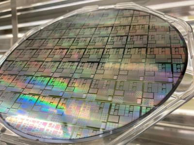
CEA-Leti and NY CREATES to co-develop STT-MRAM and SOT-MRAM devices on 300 mm wafers

Submitted by Ron Mertens on

The New York Center for Research, Economic Advancement, Technology, Engineering, and Science (NY CREATES) and CEA-Leti announced a two-year strategic R&D partnership, that will initially focus on the research and co-development of MRAM devices.

NY CREATES and CEA-Leti will develop and produce both STT-MRAM and SOT-MRAM devices on 300 mm substrates. CEA-Leti will contribute its expertise in magnetics, spintronics, and the testing of related devices, and NY CREATES will provide the facilities, process integration expertise, and materials process development to run the 300mm silicon hardware.

ITRI and TSMC announce advances in SOT-MRAM development

Submitted by Ron Mertens on

In 2022, Taiwan's Industrial Technology Research Institute (ITRI) announced an agreement with Taiwan Semiconductor Manufacturing Company (TSMC) to collaborate on SOT-MRAM R&D. ITRI and TSMC now announced that they have developed SOT-MRAM array chips that boasts a power consumption of merely one percent of a comparable STT-MRAM device. 

ITRI - TSMC SOT-MRAM array memory on wafer photo

ITRI and TSMC published a new research paper that was presented at the 2023 IEE International Electron Devices Meeting (IEDM 2023). ITRI explains that the new unit cell achieves simultaneous low power consumption and high-speed operation, reaching speeds as rapid as 10 nanoseconds. And its overall computing performance can be further enhanced when integrated with computing in memory circuit design. 

Researchers demonstrate fast BiSb p-MTJ switching, to enable fast and low-power SOT-MRAM devices

Submitted by Ron Mertens on

Researchers from the Tokyo Institute of Technology have successfully demonstrated fast p-MTJ switching (1 ns, compared to current switching that is >10 ns). "The researchers achieved this using the topological insulator BiSb as the SOT layer, and say the device offers a current density about 20 times smaller than typical.

fast low-power BiSb p-MTJ switching (Tokyo-IT)

The researchers say that this technology can be applied to develop p-MTJs for SOT-MRAM that will offer ultrafast operations and ultra low power consumption, while also offering higher reliability. This follows earlier work by the same group on BiSb p-MTJs.

Researchers say MnPd3 will enable a breakthrough in SOT-MRAM memory devices

Submitted by Ron Mertens on

Researchers from the School of Engineering at Stanford University discovered that a metallic compound called manganese palladium three MnPd3 is a promising material to build SOT-MRAM memory devices. 

Z-axes spin polarization in MnPd3

The researchers say that the new material enables a breakthrough in SOT-MRAM device performance, as it is the first material that generates spin in the z-direction, rather than the y-direction as in most materials, which is a property needed in high-performance SOT-MRAM. In fact MnPd3 is able to generate spins in any orientation because its internal structure lacks the kind of crystal symmetry that would force all of the electrons into a particular orientation.

Hprobe releases a new MRAM testing module to help increase production yields

Submitted by Ron Mertens on

Hprobe, a developer of testing equipment for magnetic devices, announced a new addition to its product line, the RF Pulse Module. The company says that this is the commercially available testing system to both collect statistics of error rate of the memory unit cell and take a deep look into switching dynamics of resistive memories.

Hprobe IBEX WAT H3DM Light photo

Hprobe's IBEX system

Hprobe says that the RF Pulse Module is two orders of magnitude faster than existing devices and can help increase manufacturing yields. Hprobe has already begun shipping to tier-1 companies and major research institutes around the world.

ITRI joins forces with TSMC and NYCU to develop next-gen MRAM technologies

Submitted by Ron Mertens on

Taiwan's Industrial Technology Research Institute (ITRI) announced two new MRAM collaborations. The first one is with Taiwan's TSMC, for the development of SOT-MRAM array chips. The second collaboration is with National Yang Ming Chiao Tung University (NYCU) to develop magnetic memory technology that can perform across a wide operating temperature range of nearly 400 degrees Celsius.

Together with TSMC, ITRI is developing low-voltage and current SOT-MRAM, that features high write efficiecny and low write voltage. ITRI says that its SOT-MRAM achieves a writing speed of 0.4 nanoseconds and a high endurance of 7 trillion reads and writes. The memory also offers a data storage lifespan of over 10 years.

ISI introduces a new 3-Axis magnet option for its MRAM tester systems, targeting STT-MRAM and SOT-MRAM testing

Submitted by Ron Mertens on

Integral Solutions International (ISI) announced a new 3-Axis Magnet Option for wafer-level testing. Combined with ISI's WLA5000 Tester, the 3D magnetic fields produced by this system can be used for characterization of MRAM devices in addition to 2D/3D Magnetic Sensors.

ISI WLA5000 MRAM tester

ISI says that for MRAM applications, the 3D Magnetic fields produced by ISI’s 3-Axis Magnet Option delivers solutions for both STT-MRAM and SOT-MRAM applications.

ITRI and UCLA to co-develop VC-MRAM technologies

Submitted by Ron Mertens on

Taiwan-based Industrial Technology Research Institute (ITRI) announced an agreement with the University of California, Los Angeles (UCLA) to co-develop Voltage-Control MRAM (VC-MRAM) technologies.

UCLA-ITRI-VC-MRAM-prototype

ITRI says that VC-MRAM is a type of SOT-MRAM that offers improved performance - 50% higher writing speed and 75% less energy consumption. VC-MRAM is said to be ideal for AIoT and automotive industry applications. The partnership is expected to strengthen the link between both parties and accelerate the R&D and industrialization of new memory technologies.

NTU and TSMC researchers develop a new SOT-MRAM structure with high spin-orbital Hall conductivity

Submitted by Ron Mertens on

Researchers from National Taiwan University in collaboration with TSMC developed a new SOT-MRAM device structure, that features sizable orbital currents. This research promises a pathway for enhancing SOT-MRAM performance by harnessing both the conventional spin currents and the emergent orbital currents.

NTU TSMC PtCr Alloys SOT-MRAM
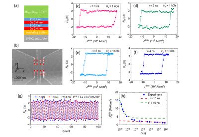
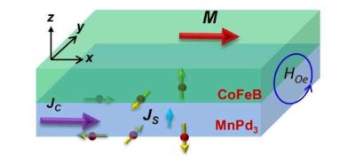
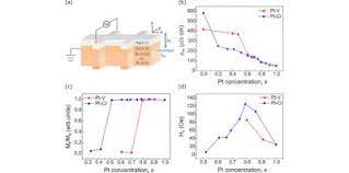
The new device is based on 3d light transition metals (such as V and Cr) that are incorporated into the classical spin Hall metal Pt. The Pt-Cr alloy enhances the charge-to-spin conversion efficiency which can realize high spin-orbital Hall conductivity, beyond the conventional spin Hall limit.

Researchers developed an ultra low power BiSb-based SOT MRAM device

Submitted by Ron Mertens on

Researchers from the Tokyo Institute of Technology developed an ultrahigh-efficiency SOT magnetization switching in fully sputtered BiSb(Co/Pt) multilayers with large perpendicular magnetic anisotropy (PMA).

Scheme of ultra low power BiSb SOT-MRAM device (Tokyo IT)

The new device offers a large spin Hall angle and high electrical conductivity, thus satisfying all the three requirements for SOT-MRAM implementation. The researchers managed to achieve robust SOT magnetization at a low current density despite the large PMA field.