Competing technologies

Researchers demonstrate a new memory device using an OLED and a MOS capacitor

Researchers from TU Dresden developed a novel memory device that is based on a combination of an light emitting material and a metal-oxide semiconductor (MOS) capacitor.

pinMOS memory structure (TU Dresden)

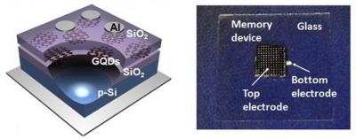
The so-called pinMOS device is a non-volatile memory-capacitor with high repeatability and reproducibility. pinMOS devices can store several states, since charges can be added or removed in controllable amounts. This device can also be controlled (read and write) both electrically and optically. The light emitting material is an OLED device.

Read the full story Posted: Dec 01,2019

Yole Developpement sees STT-MRAM leading the embedded emerging-NVM market

Market analyst firm Yole Developpement presents its latest next-generation memory forecasts in an interesting new article. The company says that following more than 15 years of development, PCM is finally taking off in stand-alone applications due to strong support from Intel and Micron.

Emerging NVM market (2018-2023, Yole)

STT-MRAM is expected to lead the embedded memory race as many foundries are rushing to add MRAM support and expertise to their product lines. STT-MRAM is promising for enterprise storage SCM.

Read the full story Posted: Dec 04,2018

Interview with Bo Hansen, CEO at Capres A/S

Bo Hansen, Capres CEOCapres A/S was established in 1999 in Denmark to develop a unique probe technology designed for in-line production monitoring in the semiconductor industry. The company, in collaboration with IBM, developed a resistivity measurement technique to characterize MTJ stacks.

Bo Svarrer Hansen, the company's CEO since 2002, was kind enough to answers a few questions we had, and share with us his views on the MRAM market and the company's measurement systems for MRAM and STT-MRAM device developers.

Q: Can you update us on Capres' current offers to the MRAM industry?

Capres customers are using our CIPTech® tools for R&D on small samples as well as volume production on 300 mm wafers. Depending on the configuration the tools measure with an in- plane or an out- of- plane magnetic field on blanket as well as patterned wafers.

Read the full story Posted: Oct 26,2016

Yole Developpement sees MRAM, RRAM and PCM memories generating $4.6 billion in 2021

Yole Developpement says that the emerging Non-Volatile Memory (NVM) market is still small, generating only $53 million in sales in 2015. The market is still limited to niche markets due to the limited densities.

Next-gen memory, time to market (Yole, 2015)

Yole sees the market growing very quickly, though, to reach $4.6 billion by 2021 - a CAGR of 110%. Yole says that the clear go-to market for emerging-NVM will be storage-class memory. High-capacity SCM applications will use either phase-change memory or RRAM memory, while applications that require high endurance and speed will adopt STT-MRAM memories.

 
Read the full story Posted: Jul 28,2016

Resistive RAM: next-gen storage memory technology

MRAM-Info has been focused on MRAM technologies for over 10 years, and the technology has advanced a lot since then, with over 60 million chips produced and growing densities. A new memory technology is now starting to enter the market as well - RRAM, or Resistive RAM, which is based on memristors, materials that change their resistance.

RRAM is promising storage-memory candidate, and we are happy to announce the launch of a new site dedicated to this technology, RRAM-Info.com. We will post daily news, commentary and updates about RRAM memory technologies. This is certainly a technology that all memory professionals should be aware of! You can subscribe to our weekly RRAM newsletter here - and if you have not done so already, be sure to also signup for our free MRAM newsletter!

Read the full story Posted: May 11,2016

Samsung will be ready with MRAM chips "soon"

Samsung's semiconductor chief Kim Ki-nam says that Samsung is developing next-generation memory technologies, such as MRAM and RRAM. According to Kim "Samsung will commercialize MRAMs and ReRAMs according to our own schedule. We are on our way and will be ready soon"

Samsung targets MRAM as an update to DRAM memory, while RRAM will be used as a storage memory to replace NAND.

Read the full story Posted: Apr 21,2016

Graphene and Tantalum enables a new kind of high-density efficient memory

Scientists at Rice University have created a solid-state memory technology based on graphene and tantalum oxide (a common insulator in electronics) that allows for high-density storage with a minimum occurrence of computer errors.

Rice scientists make graphene-tantalum solid-state memory image

The new devices require only two electrodes per circuit, making them simpler than present-day flash memories that use three. The new design is also said to require 100 times less energy than present devices. It is a new way to make nonvolatile computer memories - memories that hold their data even when the power is off, unlike volatile random-access computer memories that lose their contents when the machine is shut down.

Read the full story Posted: Aug 11,2015

More details on TDK's new 8Mb STT-MRAM prototype

A few days ago I reported that TDK will show a new STT-MRAM prototype, and now we have some more information and a couple of photos of the new test chip. TDK is showing their first STT-MRAM chip, a 8Mb device, produced on a 8" silicon substrate. 

TDK STT-MRAM wafer/chip CEATEC 2014 photo

This is the first time TDK exposed their STT-MRAM technology. Those MRAM chips were produced by TDK's Headway Technologies. TDK will not mass poroduce MRAM chips themselves but rather seek a chip-making partner to produce them. But this may take a while: TDK says it could be up to 10 years before the technology matures (earlier reports said TDK estimates that it will take 3 years to commercialize this technology).

Read the full story Posted: Oct 11,2014

Graphene Quantum Dots to enable next-gen flash memory devices

One of the problems with flash memory is that it is sensitive to defects. To solve this problem, researchers from Samsung Electronics are developing flash devices based on graphene quantum dots (GQDs). The performance of such a device is promising, with an electron density that is comparable to semiconductor and metal nanocrystal based memories. Those flash memory can also be made flexible and transparent.

The researchers used GQDs in three different sizes (6, 12, and 27 nm) between silicon dioxide layers. The memory of the QDs depend on their sizes: the 12 nm dot for example offers the highest program speed while the 27 nm dot has the highest erase speed, and is also the most stable. Samsung says that this is the first GQD demonstration in a practical device.

Read the full story Posted: Jun 19,2014