Everspin and QuickLogic sign a strategic agreement to bring MRAM technology to radiation hardened FPGAs
In 2022, Everspin Technologies signed a contract to provide MRAM technology, design, and back end of line manufacturing services to QuickLogic Corporation for a project funded by the US Department of Defense.

Today Everspin announced a new strategic contract with QuickLogic. Everspin will provide its innovative AgILYST MRAM technology, logic design, and back end of line manufacturing services to advance the development and demonstration of a Strategic Radiation Hardened (SRH) high-reliability Field Programmable Gate Array (FPGA) technology.
CEA-Leti and NY CREATES to co-develop STT-MRAM and SOT-MRAM devices on 300 mm wafers
The New York Center for Research, Economic Advancement, Technology, Engineering, and Science (NY CREATES) and CEA-Leti announced a two-year strategic R&D partnership, that will initially focus on the research and co-development of MRAM devices.
NY CREATES and CEA-Leti will develop and produce both STT-MRAM and SOT-MRAM devices on 300 mm substrates. CEA-Leti will contribute its expertise in magnetics, spintronics, and the testing of related devices, and NY CREATES will provide the facilities, process integration expertise, and materials process development to run the 300mm silicon hardware.
Numem and IC’ALPS co-develop a custom MRAM-powered AI accelerator
High-performance STT-MRAM developer Numem announced that in collaboration with ASIC/SoC designer IC’ALPS it has developed an integrated circuit with RISC-V processors, 2MBytes of NuRAM and a DSP/AI Custom Datapath Accelerator.

The two companies co-developed the SoC in an advanced technology node, taking advance of the high-performance and low power consumption of Numem's memory technology. The company also details that the physical implementation of this integrated circuit was made in a secure space (isolated location, network, and servers, and encrypted exchanges) to meet with the stringent protection of sensitive data required by this program. Numem and IC’Alps intend to extend their partnership to serve new SoC projects for customers.
Researchers report the first all-antiferromagnetic tunnel junction device with both electrical switching and electrical readout
Researchers from Northwestern University, led by Prof. Pedram Khalili, report the first all-antiferromagnetic tunnel junction (ATJ) devices with both electrical switching and electrical readout of the antiferromagnetic state. The researchers observed a large room-temperature tunneling magnetoresistance effect that is comparable in size to conventional ferromagnet-based tunnel junctions.
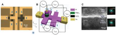
To create the new devices, the researchers used sputtering to deposit the device films on conventional silicon wafers. The films are compatible with established semiconductor manufacturing processes.
Renesas developed new STT-MRAM circuit technology, achieves the world's fastest random access speed
Renesas Electronics announced that it has developed circuit technologies for embedded STT-MRAM that reduces the energy and voltage of the memory write operation.
Renesas produced a 22-nm MCU test chip, that includes a 10.8 Mbit embedded MRAM memory cell array. It achieves a random read access frequency of over 200 MHz and a write throughput of 10.4-megabytes-per-second (MB/s).
Tohoku University researchers develop a high performance X nm MTJ
Researchers from Japan's Tohoku University developed a method to produce X nm MTJs, using a CoFeB/MgO stack structure. The researchers report that the extremely small device achieves both high-retention and high-speed. This was enabled by controlling the shape and interfacial anisotropies individually by varying the thickness of each CoFeB layer and the quantity of [CoFeB/MgO] stacks.
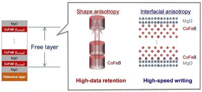
The researcher further report that shape anisotropy-enhanced MTJs showed good retention (> 10 years) at 150 °C at single nanometer sizes, whereas interfacial anisotropy-enhanced MTJs exhibited rapid speed switching (10 ns or less) below 1 V.
ITRI and TSMC announce advances in SOT-MRAM development
In 2022, Taiwan's Industrial Technology Research Institute (ITRI) announced an agreement with Taiwan Semiconductor Manufacturing Company (TSMC) to collaborate on SOT-MRAM R&D. ITRI and TSMC now announced that they have developed SOT-MRAM array chips that boasts a power consumption of merely one percent of a comparable STT-MRAM device.
ITRI and TSMC published a new research paper that was presented at the 2023 IEE International Electron Devices Meeting (IEDM 2023). ITRI explains that the new unit cell achieves simultaneous low power consumption and high-speed operation, reaching speeds as rapid as 10 nanoseconds. And its overall computing performance can be further enhanced when integrated with computing in memory circuit design.
Green Mountain Semiconductor wins a grant from NASA to develop an MRAM-enhanced neuromorphic AI processor for space applications
US-based design house and services provider Green Mountain Semiconductor (GMS) has won a Phase I Small Business Innovation Research (SBIR) contract from NASA, to develop a neuromorphic AI processor for space applications using MRAM magnetic memory.
GMS's approach involves the development of an analysis tool to optimize circuit designs for reliability and radiation resistance. This advancement will enable the use of off-the-shelf technology in space applications without the need for excessive design modifications to ensure radiation resistance.
Researchers demonstrate fast BiSb p-MTJ switching, to enable fast and low-power SOT-MRAM devices
Researchers from the Tokyo Institute of Technology have successfully demonstrated fast p-MTJ switching (1 ns, compared to current switching that is >10 ns). "The researchers achieved this using the topological insulator BiSb as the SOT layer, and say the device offers a current density about 20 times smaller than typical.
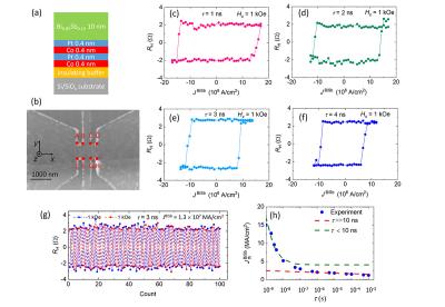
The researchers say that this technology can be applied to develop p-MTJs for SOT-MRAM that will offer ultrafast operations and ultra low power consumption, while also offering higher reliability. This follows earlier work by the same group on BiSb p-MTJs.
A recent breakthrough in spintronics research could lead to faster and more efficient optically-controlled MRAM devices
Researchers from the Hebrew University of Jerusalem in Israel have made a recent discovery that could change the face of spintronics research - the most important equation used to describe magnetization dynamics, namely the Landau-Lifshitz-Gilbert (LLG) equation, also applies to the optical domain.
A spintronics device developed by Professor Capua's lab
The new discovery has relevant applications in optical magnetic recording, namely in optically-controlled MRAM technology. Manipulation of the magnetization order parameter on optical timescales is key for ultrafast spintronics, which allows for faster, energy-efficient optically-controlled MRAM technology.