Samsung researchers update on the company's 14 nm eMRAM project

Researchers from Samsung will soon present at IEDM 2022 a new research paper that will discuss the company's latest achievements in scaling down its MRAM technology to the company's 14nm FinFET logic process.

Samsung eMRAM image

The Samsung researchers produced a stand-alone memory with a write energy requirement of 25 pJ per bit and active power requirements of 14 mW for reading and 27 mW for writing at a 54Mbyte per second data rate. The cycling  is 10^14 cycles and when scaled to a 16Mbit device, a chip would occupy 30 square millimeters.

Read the full story Posted: Oct 26,2022

ITRI joins forces with TSMC and NYCU to develop next-gen MRAM technologies

Taiwan's Industrial Technology Research Institute (ITRI) announced two new MRAM collaborations. The first one is with Taiwan's TSMC, for the development of SOT-MRAM array chips. The second collaboration is with National Yang Ming Chiao Tung University (NYCU) to develop magnetic memory technology that can perform across a wide operating temperature range of nearly 400 degrees Celsius.

Together with TSMC, ITRI is developing low-voltage and current SOT-MRAM, that features high write efficiecny and low write voltage. ITRI says that its SOT-MRAM achieves a writing speed of 0.4 nanoseconds and a high endurance of 7 trillion reads and writes. The memory also offers a data storage lifespan of over 10 years.

Read the full story Posted: Jun 28,2022

Renesas develops 22-nm circuit technologies for embedded STT-MRAM

Renesas announced that it has developed 22-nm embedded STT-MRAM circuit technologies. Renesas developed a test 32-megabit (Mbit) chip with an embedded MRAM memory cell array that achieves 5.9-nanosecond (ns) random read access at a maximum junction temperature of 150°C, and a write throughput of 5.8-megabyte-per-second (MB/s).

To achieve this performance, Renesas developed two technologies. The first is a fast read technology employing high-precision sense amplifier circuit, utilizing capacitive coupling. The second is a fast write technology, with simultaneous write bit number optimization and shortened mode transition time.

Read the full story Posted: Jun 18,2022

Researchers demonstrate an ultra-fast and efficient laser-induced opto-MRAM device

Researchers from Eindhoven University of Technology (TU/e) and the Fert Beijing Institute of Beihang University have experimentally demonstrated a fully-functional picosecond opto-MRAM building block device, by integrating ultrafast photonics with spintronics.

The researchers used a femtosecond (fs) laser, which is the fastest stimuli commercially that enabled the device to be extremely fast - and also a thousand times more energy efficient compared to standard MRAM devices. The device is based on the femtosecond laser-induced all-optical switching (AOS) scheme in synthetic ferrimagnetic multilayers that was discovered by TU/e in 2017, integrating it with MRAM bit

Read the full story Posted: Apr 30,2022

ITRI and UCLA to co-develop VC-MRAM technologies

Taiwan-based Industrial Technology Research Institute (ITRI) announced an agreement with the University of California, Los Angeles (UCLA) to co-develop Voltage-Control MRAM (VC-MRAM) technologies.

UCLA-ITRI-VC-MRAM-prototype

ITRI says that VC-MRAM is a type of SOT-MRAM that offers improved performance - 50% higher writing speed and 75% less energy consumption. VC-MRAM is said to be ideal for AIoT and automotive industry applications. The partnership is expected to strengthen the link between both parties and accelerate the R&D and industrialization of new memory technologies.

Read the full story Posted: Mar 04,2022

NTU and TSMC researchers develop a new SOT-MRAM structure with high spin-orbital Hall conductivity

Researchers from National Taiwan University in collaboration with TSMC developed a new SOT-MRAM device structure, that features sizable orbital currents. This research promises a pathway for enhancing SOT-MRAM performance by harnessing both the conventional spin currents and the emergent orbital currents.

NTU TSMC PtCr Alloys SOT-MRAM
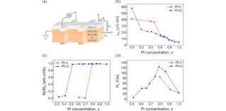
The new device is based on 3d light transition metals (such as V and Cr) that are incorporated into the classical spin Hall metal Pt. The Pt-Cr alloy enhances the charge-to-spin conversion efficiency which can realize high spin-orbital Hall conductivity, beyond the conventional spin Hall limit.

Read the full story Posted: Feb 27,2022

Researchers developed an ultra low power BiSb-based SOT MRAM device

Researchers from the Tokyo Institute of Technology developed an ultrahigh-efficiency SOT magnetization switching in fully sputtered BiSb(Co/Pt) multilayers with large perpendicular magnetic anisotropy (PMA).

Scheme of ultra low power BiSb SOT-MRAM device (Tokyo IT)

The new device offers a large spin Hall angle and high electrical conductivity, thus satisfying all the three requirements for SOT-MRAM implementation. The researchers managed to achieve robust SOT magnetization at a low current density despite the large PMA field.

Read the full story Posted: Feb 23,2022

Samsung researchers are first to demonstrate MRAM-based in-memory computing

Researchers from Samsung's Advanced Institute of Technology (SAIT), have demonstrated what they say is the world’s first in-memory computing based on MRAM, targeting next-generation AI chips.

The researchers explain that In-Memory computing is a new paradigm that seeks to perform both data storage and data computing in a memory network. In such a computing system, a large amount of data, stored in the memory network, can be executed in a highly parallel manner. Power consumption in such systems is substantially reduced.

Read the full story Posted: Jan 13,2022

Researchers use MIFL to increase the magnetoresistance of pMTJs

Researchers from the University of Arizona developed a new pMTJ structure that exhibits high magnetoresistance, strong retention and is likely to achieve fast switching times as well.

pMTJ with multi-interface free layer (Arizona University)

The new structure uses a multi-interface free layer (MIFL) which incorporate multiple materials with different properties. The researchers used a ferromagnetic CoFeB layer with nonmagnetic Mo or MgO layers. The magnetoresistance can be controlled by changing the thickness of the CoFeB layer. The researchers managed to demonstrate a magnetoresistance of over 200%.

Read the full story Posted: Dec 31,2021