 Micromem is pleased to announce another major milestone has been met in the manufacturing of their MRAM. Based on this early success the foundry has been authorized to assemble the complete memory structure.
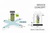
 The Hall Sensor forms an integral component of the Micromem MRAM design. The Hall Sensor is used to measure the external field of a magnet whose magnetization can be reversed by generating a current in a coil.
 Several Hall Cross sensor devices were manufactured at various features sizes as we drive the overall MRAM cell feature size to the limits of the GCS foundry. Micromem successfully manufactured and tested a Hall Cross Sensor device that functions precisely in accordance with the University of Toronto sensitivity model, notably the following:   - The sensor demonstrates excellent linearity
   - The magnetic field reversal yields symmetrical V(Hall) within
      expected tolerances
   - I (bias) reversal yields symmetrical V(Hall) within expected
      tolerances.
"What this means for the foundry phase is that Micromem's Hall Cross Sensor device is extremely accurate, repeatable and linear, all necessary features for a memory design. The results have exceeded our expectations. As a result of the tremendous performance, we plan to also use the Hall Cross Sensor devices as credible on-wafer sensors to evaluate our optimization efforts for the placement of the magnetic yoke structures," says Steve Van Fleet, Project Director.
Having exceeded the test requirements on the Hall Cross Sensor device, we have authorized the foundry to accelerate their efforts on the complete MRAM cell manufacturing. We will have an additional update on actual memory cell testing prior to December 25, 2007.
As a result of this positive test data we have defined the first MRAM array sizes that we are targeting. These have been defined in concert with some of our interested end users who will ultimately utilize our memory. Our initial target MRAM array sizes are 40 bits, 256 bit, 512 bits and 1024 bits. In addition to these high-speed memory size requirements, we have been requested to design to a 16K bit memory array of low speed embedded memory. This will be used for identification purposes only where radiation hardened is the key parameter and typically high speed memory read write time is not critical.
Micromem continues to meet and or exceed the foundry targets. Management is committed to our investors to provide timely and informative press releases as we march the company towards full commercialization.
Â