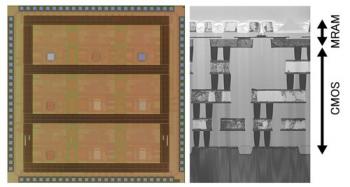
NEC

NEC and Tohoku University developed MRAM based spin-CAM

NEC Corporation and Tohoku University have developed an MRAM based CAM (content addressable memory) that includes non-volatile storage by using the vertical magnetization of vertical domain wall elements in a cobalt-nickel active layer. They call this Spin-CAM.

NEC and Tohoku built a 16-kbit Spin-CAM prototype chip (using a 90-nm process). This chip features 5 ns search cycle time, 200-microamps write current and a 6.6 square micron memory cell. Such a CAM may be used to create instant-on electronics and zero-electricity standby modes.

Read the full story Posted: Jun 13,2011

NEC says that using their MRAM-based magnetic flip flop can help make low power standby mode

There's an interesting article at Tech-On, by NEC, on their MRAM-based magnetic flip flip (MFF). NEC say that using such flip-flops can make low power  'standby' mode for appliances (TVs, computers, portable devices...).

Today, for example, LCD TVs have two kinds of standby - "fast standby" which consumes as much as 15W, and 'slow standby' that may consume as low as 0.1W, but may take a few seconds to show a picture when powered back on. The MFF might make it possible to design a stand-by mode that is both fast to power on, and uses minimal power.

Read the full story Posted: Jul 26,2009

NEC to commercialize perpendicular MRAM chips in 2010

A couple of days ago we reported that NEC are working towards perpendicular MRAM using 2T1MTJ... now we have some more info, thanks to TechOn.

NEC and NEC Electronics employed a new method called "spin torque domain wall displacement write method" to reduce write current and realize microfabrication at the same time. In fact, they aim to reduce the current by as much as 90%. They were also able to increase speed to 500Mhz. This technology is not 'new', it was announced in 2007, but now they have a test chip ready.

Read the full story Posted: Jun 17,2009

NEC developed perpendicular STT-RAM technology

NEC announced that they have developed the world's first STT-MRAM with current-induced domain wall motion using perpendicular magnetic anisotropy material. Perpendicular magnetic anisotropy enables a cell to carry out the current-induced domain wall motion writing method using spin torque at a low current, which leads to easy scaling down of cell size and creates suitable conditions for next generation system LSI.

The newly developed current-induced domain wall motion writing method, using spin torque and perpendicular magnetization material, is capable of reducing current while writing for a scaled down cell beyond the 55 nanometer process.

Read the full story Posted: Jun 15,2009

NEC Develops 32Mb Embeddable MRAM

NEC announced the successful operational demonstration of a 32Mb MRAM that can be embedded in SoCs. NEC has reduced the area of control circuits in the 32Mb MRAM design in order to achieve superior cell efficiency that enables 73% of a memory macro's area to be allocated to memory cells. This was achieved by developing write circuits, which enables greater memory capacity.  The high-speed cycle time of 9ns was achieved by adopting new decoder circuits that minimize delay.

Furthermore, compatibility with an asynchronous SRAM was achieved by inserting protocol transform circuits between the MRAM macro and I/O buffer circuits.

In November 2007 NEC developed a high speed 250MHz, 1Mb MRAM macro suitable for embedding in system LSIs. However, since the memory cell of the high speed 1Mb MRAM macro consists of two transistors and one MTJ, enlarging its memory capacity is more challenging than increasing the memory of MRAM macro equipped with just one transistor and one MTJ cell.

The latest demonstrations adapted MRAM macro cell arrays with NEC's newly developed write circuits to achieve macro cell efficiency of 73%. This both reduced MRAM macro size and enlarged memory capacity.

The macro's word line decoder circuit was equipped with a word boost circuit in order to shrink memory cell area. However, word boost circuits are prone to delay and tend to extend the cycle time of macros. To solve this problem, a word boost circuit featuring optimized conversion levels was developed. Accordingly, the high speed operation cycle time of 9ns was achieved despite being a large capacity 32Mb macro.

Looking forward, NEC is aiming to demonstrate an SoC integrated with large capacity, high speed MRAM macros.
Read the full story Posted: Feb 12,2009

NEC makes magnetic flip flops

NEC has announced it managed to make a 1-bit Magnetic Flip Flop (MFF, as they like to call it). Unlike existing flip-flops, it does not need power to retain the value.
NEC suggests using such flip-flops instead of regular ones, and using MRAM instead of SRAM and you can make a system on a chip that does not need power to store data. MRAM is better than FLASH, says NEC, because of the unlimited write cycles.
NEC's MFF opereates at 1.2V or less, like regular flip-flops. The clock speed can be up to 3.5GHz.

Read the full story Posted: Jan 05,2009

NEC Develops World's Fastest SRAM-Compatible MRAM With Operation Speed of 250MHz

NEC Corporation announced that it has succeeded in developing a new SRAM-compatible MRAM that can operate at 250MHz, the world's fastest MRAM operation speed. MRAM is expected to be the dominant next-generation memory technology as it realizes ultra fast operation speeds, nonvolatility - ability to retain data with the power off, and unlimited write endurance.

Verification at the SRAM speed level proves that the newly-developed MRAM could be embedded in system LSIs as SRAM substitutes in the future.

The unique MRAM was designed and fabricated by NEC and has a memory capacity of 1 megabit. Incorporating a memory cell with two transistors, one magnetic tunnel junction, and a newly-developed circuit scheme, the new design achieves an operation speed of 250MHz; double that of conventional MRAMs and almost equivalent to that of recent LSI-embedded SRAM.

Read the full story Posted: Nov 30,2007

Toshiba and NEC Develop World's Fastest, Highest Density MRAM

Toshiba Corporation and NEC Corporation today announced that they have developed a magnetoresistive random access memory (MRAM) that combines the highest density with the fastest read and write speed yet achieved. The new MRAM achieves a 16-megabit density and a read and write speed of 200-megabytes a second, and also secures low voltage operation of 1.8V.
A major challenge of MRAM development to date has been the acceleration of read speeds: the current drive circuit used to generate the magnetic field for writing degrades read operation from memory cells. The new MRAM has an improved circuit design that divides the current paths for reading and writing, realizing a faster read speed. It also reduces equivalent resistance in wiring by approximately 38% by forking the write current. These innovations together achieve a read and write speed of 200-megabytes a second and a cycle time of 34 nanoseconds — both the world's best performance for MRAM. This performance is underlined by a low operating voltage of only 1.8V, the ideal voltage for mobile digital products.
Alongside advances in performance, the new MRAM achieves advances in chip size. Toshiba and NEC have introduced the above mentioned technologies and optimized overall circuit design, achieving a chip that, at 78.7mm2, is approximately 30% smaller than its equivalent without the new circuit design. The new MRAM is the world's smallest in the 16-megabit era.

Read more here 

Read the full story Posted: Feb 07,2006

Canon buys Anelva Corp

In an effort to someday profit off of the manufacturer of surface-conduction electron-emitter display or SED devices, Canon yesterday bought 53.9% of NEC Machinery and all of NEC Machinery’s shares in Anelva Corp., a subsidiary of NEC Corp. Anelva is a japanese company that manufactures major equipment for the fabrication of semiconductors and LCDs using vacuum technology. Anelva developed a 200- to 300-mm-wafer-compliant deposition (sputtering) equipment for MRAM, the C-7100, using their unique low-pressure plasma deposition technique.

Read the full story Posted: Oct 05,2005

New MRAM technologies are the spotlight at the VLSI 2005 symposium

MRAM has been considered as a potential next-gen memory technology for quite some time, and it was in the spotlight at the VLSI 2005 symposium. NEC and Toshiba jointly unveiled a new Toggle MRAM cell structure in which the magnetic tunnel junction has a multi-layered structured.

Fujitsu Laboratories presented a new approach to MRAM circuity. The company is developing embedded MRAM and they have now proposed a one-transistor/two-magnetic tunnel junction (1T/2MTJ) structure MRAM cell with a direct voltage-sensing scheme, which it said has the advantages of DRAMs. In the proposed 1T/2MTJ cell, two MTJs were connected in series. Fujitsu fabricated the test device with each MTJ measuring 0.2 x 0.4 micron and confirmed the cell operation.

Read the full story Posted: Jun 20,2005