August 2005

World's first radiation-hardened and tolerant MCU that can interface with Honeywell's MRAM

Silicon Laude announces the availability of the world’s first, and only, radiation-hardened and radiation-tolerant MCS8051 instruction-compatible microcontrollers that can directly interface with Honeywell’s new HXNV-0100 64k x 16 radiation-hardened Magnetic RAM (MRAM), yielding an unprecedented two-chip, radiation-hardened/tolerant microcontroller solution capable of reliable operation in 300 krads (Si) total ionizing-dose (TID) environments.

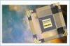
Dubbed the SL80RT051-AX001 for the radiation-tolerant version, and SL80RH051-AF001 for the radiation-hardened version (or SL80RX051 collectively), the microcontrollers are implemented in Actel space-qualified RTAX-S and Aeroflex radiation-hardened UT6325 FPGAs (respectively). SL80RX051 applications include, among others, general instrumentation and control, launch vehicle vibration monitoring, Tunable Diode Laser (TDL) spectrometers, and general data acquisition functions. Because of the MRAM’ s non-volatile storage capability, the MRAM/SL80RX051 combination is ideal for applications that need to collect and store data periodically, with later, less frequent uploads. Another advantage to the MRAM approach is that programs can be easily updated due to the fact that data and programs can be written to the MRAM like ordinary SRAM, but retained like an EEPROM when powered down. To prevent unintended writes to program memory, the SL80RX051 includes a write protection security lock that can be deactivated with a unique, three-byte code and enable sequence, similar to an ordinary flash memory.

Read the full story Posted: Aug 22,2005

Research and Markets : MRAM is the First Radically New Memory Technology to Show Real Commercial Promise for Many Years

Research and Markets has announced the addition of Magneto resistive Random Access Memories (MRAM) Summary to their offering.

MRAM is the first radically new memory technology to show real commercial promise for many years. This report summarizes the extensive market research that has been done in the MRAM market and extends the coverage of MRAM provided in the Emerging Memory Technologies report. MRAM is already being commercialized and this report examines why MRAM is becoming one of the first complex nano-engineered products to hit the marketplace. It also takes a look at the challenges that this technology faces and provides a table indicating which market sectors are likely to use MRAM and when, and what their reasons for adoption would be. Sectors covered include mobile computing, cell phones and other handhelds, portable recording and other playback devices, home computing and consumer electronics, enterprise computing and telecommunications, control systems and embedded computing, and disposable electronics. Another table reviews the activities of approximately 15 actual and likely suppliers of MRAM including both giants, such as Freescale, and less well-known start-ups. The report ends with an analysis of the available marketing strategies in the MRAM market and a forecast of MRAM revenues over the next eight years.

Read the full story Posted: Aug 03,2005

MRAM record: memory cell runs at 2 GHz

Up to now, the read/write speeds only amounted to a few 100 MHz because the precession of the spins is very slow. Now, Hans Schumacher of the German Physical-Technical Institute in Braunschweig (PTB) has shown how this can be done faster: Very short impulses address the memory cell, adjusting the spin by 180 or 360° instead of precessing. Others have also had this idea, but the problem always was that the process only worked in one cell -- one bit -- and not in realistic memory chips in which multiple cells are addressed in one matrix. The short, but strong electric impulse affects neighboring cells.
Schumacher has now managed to develop a special series of pulses to solve this problem; he calls it "ballistic addressing." The step from the research lab to the development laboratory will reveal whether this new approach will make MRAM market-ready. Time is crucial, for the cells cannot keep getting smaller. They are now approaching what is called the superparamagnetic limit, above which a magnetic element is no longer constantly remagnetized by thermal energy. A smaller cell would not have any remanence and could therefore not be used as a storage module. Depending on the material used, this limit is around 10 nm -- in an area that lithography techniques should reach in about 15 years according to the semiconductor roadmap. In light of this deadline, MRAM proponents will have to produce a working product as quickly as possible.

Read more here 

Read the full story Posted: Aug 01,2005