Toshiba

Toshiba and Hynix prototype a 4 Gb STT-MRAM

Toshiba and SK Hynix co-developed a 4-Gbit STT-MRAM chip, and presented a prototype at IEDM 2016.

Toshiba Hynix 4Gb STT-MRAM mTJ array photo

The prototype chip is made from eight 512-Mbit banks, and the cell area is equivalent to that of DRAM - at 9F2, which Hynix says is much smaller than conventional STT-MRAMs (50F2).

Read the full story Posted: Dec 20,2016

Toshiba shows a new STT-MRAM test chip that consumes about 80% less power than SRAM memory

Toshiba presented a new STT-MRAM 1-Mb test chip that provides speed performance capable of 3.3-ns access to in-cache memory. The newly developed circuit consumes about 80% less power compared to a conventional SRAM as embedded memory - and Toshiba says that this makes it the best power-performing embedded memory.

Toshiba STT-MRAM test chip (Feb 2015)

To make this chip, Toshiba developed a new class of magnetic materials, that enabled them to build this low-power, high-efficiency, high-speed performance in energy-efficient magnetic tunnel junction (MTJ) memory.

Read the full story Posted: Mar 07,2015

Toshiba developed STT-MRAM based microprocessor cache memory

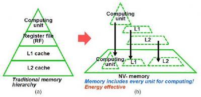
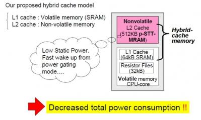
Toshiba developed new STT-MRAM technology that can be used to enable MRAM based cache memory for microprocessors. The L2 cache alone uses about 80% of the power consumed by the CPU, so reducing the power consumption of the cache is very important - and STT-MRAM may reduce this consumption by about 60%. It's not clear how close is this technology to actually being commercialized.

Toshiba's new STT-MRAM uses a dual-cell (2T-2MTJ) circuit in which the two MTJs have complementary resistive states (high and low resistive states). This eliminates the leak path and also increases the readout signal intensity - and so improves access speed. In Toshiba's cahce, the read time is 4.1 ns - very close to that of SRAM, while the write time (2.1ns) is similar to SRAM. Toshiba also implemented error correction mechanisms into the cache STT-MRAM chip.

Read the full story Posted: Jun 12,2014

Toshiba's new STT-MRAM based computing architecture to enable drastically faster and more efficient CPUs

Toshiba announced a new computing architecture that uses only STT-MRAM to perform both operations and storage. The idea support computing capability, register file, primary cache and secondary cache all on the same perpendicular STT-MRAM, and Toshiba says it could lead to CPUs that are drastically faster and more efficient.

Toshiba explains that in the new architecture, the results of operations (answers) that correspond to combinations of certain inputs are prepared in advance in the form of a table and stored in the memory. In response to an input, an answer is read out of the memory. This is equivalent to an operation carried out by a CPU. Because the computation answer is read once, it drastically improves processing speed and power consumption.

Read the full story Posted: Dec 12,2013

Toshiba developed the lowest power consumption STT-MRAM memory element, will accelerate R&D

Toshiba has developed a prototype memory element for STT-MRAM that (according to Toshiba) achieves the world's lowest power consumption yet reported. STT-MRAM based on this element has the potential to surpass the power consumption efficiency of SRAM as cache memory.

Toshiba's improved structure is based on perpendicular magnetization and takes element miniaturization to below 30nm. Introduction of this newly designed "normally-off" memory circuit with no passes for current to leak into cuts leak current to zero in both operation and standby without any specific power supply management. The company says it improved the speed of their previous design - while reducing the power consumption by 90%.

Read the full story Posted: Dec 10,2012

Toshiba seeks a joint MRAM project at Elpida's DRAM fab

There are reports that Toshiba decided not to bid in the corporate rehabilitation efforts of Elpida Memory. But Toshiba does plan to offer a joint MRAM project to whoever takes over Elpida's DRAM factory in Japan. Toshiba is already collaborating with Hynix on MRAM.

It is expected that two companies will bid (this is the second round of bidding) - Micron Technology (who are developing STT-MRAM together with A*STAR) and a joint bid by the US investment fund TPG Capital and a fund under the Lenovo Group.

Read the full story Posted: Apr 27,2012

Toshiba designed an STT-MRAM/SRAM hybrid cache for ultra-low power processors

Toshiba has a new hybrid cache design that uses STT-MRAM and SRAM combination. This is aimed towards next-generation low-power computer processors. These new computers will usually be off, and the time and power it takes to "wake up" is considerable. The new design can reduce the energy consumption by around half - and does not effect processing capacity.

Toshiba's design uses a 512Kb STT-MRAM cache combined with a 32Kb register file and a 64Kb SRAM primary cache. Using the non-volatile MRAM, the power gating can be conducted more frequently. In current designs, it takes around 20 micro seconds to recover from power gating and about 150 micro seconds from deep-sleep mode. In the new design, it takes only 1 micro second to recover from power gating.

Read the full story Posted: Nov 08,2011

Toshiba to use MRAM as cache for HDD and NAND

Kiyoshi Kobayashi, president of Toshiba's Semiconductor and Storage Products Company, said that "MRAMs will make it possible to take further advantage of NAND flash memories and HDDs, whose access performances are low,". It seems that Toshiba plans to use MRAM as cache for both NAND and HDDs devices.

Toshiba hasn't given up on the idea of having a full MRAM memory device - replacing HDD/NAND/DRAM altogether, but using it as a cache can be a step towards this goal.

Read the full story Posted: Aug 17,2011

Toshiba and Hynix to co-develop and produce MRAM products

Toshiba and Hynix announced an agreement to jointly develop MRAM products. Once the development is complete, the companies intend to establish an MRAM production plant together. We believe the companies intend to develop STT-MRAM technology.

Toshiba has been developing STT-MRAM for quite some time, and just a few days ago reported a breakthrough MTJ device that could pave the way towards Gigabit MRAM devices. They expect such chips within 3-4 years, so that's probably the same time frame on the new JV with Hynix.

Read the full story Posted: Jul 13,2011

Toshiba report STT-MRAM advances, expects gigabit chips within 3-4 years, to be cost competitive to DRAM

Toshiba says that their newly developed perpendicular magnetization-type magnetic tunnel junction (MTJ) device has excellent properties - and it can be a basic element towards a gigabit STT-MRAM device. The company says that these 'research results' are encouraging and they will now shift to the development of products. Commercialization of gigabit STT-MRAM is expected within 3 to 4 years.

MTJ cross section (Toshiba)MTJ cross section (Toshiba)

The device's writing current density is 5 x 10⁵Acm-2, which is 1/6 that of the company's existing products. And its magnetic resistance (MR), which determines data reading margin, is 200%, which was drastically improved from the 15% of the existing products. Toshiba managed to have both a low writing current density and a high MR ratio by using cobalt and iron based materials for the recording layer.

Read the full story Posted: Jul 06,2011