
Avalanche Technology adds new 2Gb and 8Gb densities of its 3rd-Gen space-grade STT-MRAM

Submitted by Ron Mertens on

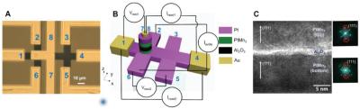
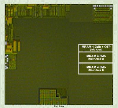
pMTJ STT-MRAM developer Avalanche Technology launched two new densities of its 3rd generation space-grade parallel asynchronous x32-interface high-reliability P-SRAM (Persistent SRAM) memory devices, based on its latest STT-MRAM tech, in 2Gb and 8Gb.

In June 2023 Avalanche announced that it is providing its products for satellite power applications developed by Advanced Space Power Equipment. Earlier that year Avalanche announced that its Gen-3 Space Grade Dual QSPI solution is now available in pre-production.

Researchers report the first all-antiferromagnetic tunnel junction device with both electrical switching and electrical readout

Submitted by Ron Mertens on

Researchers from Northwestern University, led by Prof. Pedram Khalili, report the first all-antiferromagnetic tunnel junction (ATJ) devices with both electrical switching and electrical readout of the antiferromagnetic state. The researchers observed a large room-temperature tunneling magnetoresistance effect that is comparable in size to conventional ferromagnet-based tunnel junctions. 

Northwestern Uni: Electrically-Controlled All-Antiferromagnetic Tunnel Junctions on Silicon image

To create the new devices, the researchers used sputtering to deposit the device films on conventional silicon wafers. The films are compatible with established semiconductor manufacturing processes. 

Tiempro Secure's Secure Element succesfully implemented in GlobalFroundries 22-nm process with MRAM memory

Submitted by Ron Mertens on

France-based Tiempro Secure announced that its TESIC RISC-V Secure Element was implemented in GlobalFoundries’ 22-nm platform with embedded MRAM, after a rigorous characterization process.

Tiempo Secure says it leveraged its long-standing know-how in Secure IP, to adapt its TESIC  design to the 22FDX technology process node. The TESIC platform has a secure architecture based on a RISC-V CPU core, several memory types (including ROM, RAM, Cache,  Crypto-RAM, and MRAM), random number generators, security  sensors, and secure crypto-accelerators. This provides a pre-silicon  certified IP solution on GF’s 22FDX to SoC manufacturers who require a high-end Secure  Element.

Everspin hopes to get US government support to expand its 200 mm MRAM production capacity

Submitted by Ron Mertens on

Everspin Technologies announced that it has applied for the CHIPS Incentives Program, asking for funding for an additional 200mm MRAM production line. Everspin says the new funding will help it increase its long-term R&D IP capability. 

Everspin Technologies chip photo

In November 2022, Everspin asked for funding to build a new MRAM production line in Indiana.

Everspin reports its Q4 2023 earning results

Submitted by Ron Mertens on

Everspin Technologies reported its financial results for Q4 2023, with revenues of $16.7 million and a net income of $2 million. Product sales were a bit slower than last year, but licensing and royalties were higher at $4.3 million (up from $1.1 million in 2022).


Everspin chip render

For the full year 2023, Everspin achieved record revenues of $63.8 million (up 6% from 2022), and net income of $9.1 million. At the end of the year Everspin had a cash balance of $36.9 million.

Renesas developed new STT-MRAM circuit technology, achieves the world's fastest random access speed

Submitted by Ron Mertens on

Renesas Electronics announced that it has developed circuit technologies for embedded STT-MRAM that reduces the energy and voltage of the memory write operation. 

Renesas embedded 22nm STT-MRAM test chip photo

Renesas produced a 22-nm MCU test chip, that includes a 10.8 Mbit embedded MRAM memory cell array. It achieves a random read access frequency of over 200 MHz and a write throughput of 10.4-megabytes-per-second (MB/s).

PSMC collaborates with Power Spin for MRAM production by 2029

Submitted by Ron Mertens on

Reports in Japan suggest that Taiwan's Powerchip Semiconductor Manufacturing (PSMC) will enter into a new MRAM R&D project, together with Japan's Power Spin. PSMC plans to start producing MRAM chips by 2029, at its 12-inch factory that it is now building in Japan.

Power Spin, that holds MRAM IP originally developed at Tohoku University, will license its IP to PSMC and will assist in the required R&D and ramp-up of production at PSMC's fab. PSMC looks to utilize the MRAM technology mainly for generative AI data center solutions.

Tohoku University researchers develop a high performance X nm MTJ

Submitted by Ron Mertens on

Researchers from Japan's Tohoku University developed a method to produce X nm MTJs, using a CoFeB/MgO stack structure. The researchers report that the extremely small device achieves both high-retention and high-speed. This was enabled by controlling the shape and interfacial anisotropies individually by varying the thickness of each CoFeB layer and the quantity of [CoFeB/MgO] stacks.

single-nanometer MTJ structure, Tohoku University

The researcher further report that shape anisotropy-enhanced MTJs showed good retention (> 10 years) at 150 °C at single nanometer sizes, whereas interfacial anisotropy-enhanced MTJs exhibited rapid speed switching (10 ns or less) below 1 V.

ITRI and TSMC announce advances in SOT-MRAM development

Submitted by Ron Mertens on

In 2022, Taiwan's Industrial Technology Research Institute (ITRI) announced an agreement with Taiwan Semiconductor Manufacturing Company (TSMC) to collaborate on SOT-MRAM R&D. ITRI and TSMC now announced that they have developed SOT-MRAM array chips that boasts a power consumption of merely one percent of a comparable STT-MRAM device. 

ITRI - TSMC SOT-MRAM array memory on wafer photo

ITRI and TSMC published a new research paper that was presented at the 2023 IEE International Electron Devices Meeting (IEDM 2023). ITRI explains that the new unit cell achieves simultaneous low power consumption and high-speed operation, reaching speeds as rapid as 10 nanoseconds. And its overall computing performance can be further enhanced when integrated with computing in memory circuit design. 

Netsol Unveils First Standalone MRAM Using 28nm Process, Shares the Outlook for Standalone MRAM at 2023 MRAM Forum

Submitted by Ron Mertens on

At the 2023 MRAM Forum, a key event by the IEEE Magnetics Society tied to the IEDM conference, Mr. Noh, Chief Technology Officer at Netsol, provided an overview of the company's advancements in MRAM technology.

IEE MRAM Forum 2023 - Netsol presentation

Mr. Noh introduced Netsol's development of its first standalone MRAM, created using 28nm eMRAM technology from Samsung Foundry. He presented the technical characteristics of the product, focusing on its data retention, endurance,  resistance to magnetic interference and quality, which have been validated through extensive testing.