Researchers add YSZ layers to MRAM devices to increase efficiency and speed

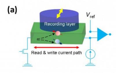
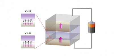
Researchers from the Korea Institute of Science and Technology (KIST) have managed to drastically incraese the speed of MRAM devices while reducing the power consumption by adding a layer of yttria-stabilized zirconia (YSZ) to MRAM devices.
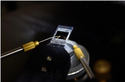
KIST ultra-low power and high-speed MRAM prototype

The YSZ layer, which has high ion conductivity helps inject hydrogen ions into the MRAM cell. This resulted in an increase in the speed of the spin alignment direction changes 100-fold.
Read the full story Posted: May 28,2020

Successful MRAM Production Requires Good Magnetic Test Equipment

This is a sponsored post by Integral Solutions Int'l

MRAM is likely to be the most promising next-generation non-volatile memory technology today. Toggle MRAM and STT-MRAM are already entering the market, gaining market share in many applications. Next-generation MRAM technologies, such as SOT-MRAM could enable the replacement of even the fastest SRAM applications, with higher densities.

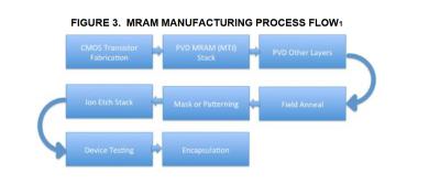
MRAM Manufacturing Process Flow (Coughlin)Source: Coughlin Associates, 2019

The MRAM production process has many stages, as device architecture is relatively complex, with a magnetic cell (frontplane) fabricated on top of a CMOS backplane. (use Figure 2 or Figure 3 from Coughlin). Measurement and characterization of devices are highly important, and the production of MRAM memories depend on measurement tools are are specialized for MRAM and STT-MRAM measurements.

Read the full story Posted: May 26,2020

New research may hold the key towards antiferromagnetic MRAM

Researchers from the University of Arizona discovered that in common Magnetic Tunnel Junctions (MTJ), there's a thin (2D) layer of Iron Oxide. This layer was found to act as a contaminant which lowers the performance achieved by MTJs, but it may also hold the key to use antiferromagnetism in MRAM devices.

Magnetic Tunnel Junction schematic (UArizona)

The researchers discovered that the layer behaves as a so-called antiferromagnet at extremely cold temperatures (below -245 degrees Celsius). Antiferromagnets are promising as these can be manipulated at Terahertz frequencies, about 1,000 times faster than existing, silicon-based technology. This is the first research that shows how Antiferromagnets can be controlled as part of MTJs and in the future may pave the way for its adoption in MRAM devices.

Read the full story Posted: May 13,2020

Researchers show how antiferromagnetic STT-MRAM technology can enable higher-density and lower energy memory

Researchers from Northwestern University suggest building STT-MRAM devices from antiferromagnetic materials - as opposed to the currently-used ferromagnetic ones. The researchers say that these materials will enable higher-density devices that feature high speed writing with low currents.

Antiferromagnetic materials are magnetically ordered at the microscopic scale, but not at the macroscopic scale. This means that there is no magnetic force between adjacent bits in MRAM cells built from these materials - which means you can pack them very close together.

Read the full story Posted: Feb 21,2020

Researchers demonstrate that chalcogenide materials can be highly suitable for SOT-MRAM

Researchers from National Taiwan University demonstrate that chalcogenide material BiTe with non-epitaxial structure can give rise to a giant spin Hall ratio and SOT efficiency (~ 200%) without obvious evidence of topologically-protected surface state (TSS).

BiTe material system for SOT-MRAM schema (NUS)

The researchers explain that a clear thickness-dependent increase of the SOT efficiency indicates that the origin of this effect is from the bulk spin-orbit interaction of such materials system. Efficient current-induced switching through SOT is also demonstrated with a low zero-thermal critical switching current density (~ 6×10⁵ A/cm2).

Read the full story Posted: Feb 18,2020

New USMR MRAM structure promises extremly simple design

Researchers from Tokyo's Institute of Technology (Tokyo Tech) developed a new MRAM cell structure (called USMR MRAM) that features a very simple structure with only two layers - which could hopefully enable lower-cost MRAM devices.

USMR MRAM cell structure image

The new design uses a combination of a topological insulator with a ferromagnetic semiconductor which enables a giant unidirectional spin Hall magnetoresistance (USMR).

Read the full story Posted: Dec 29,2019

New super-lattice SL-STT-MRAM enable faster and more efficient memory architecture

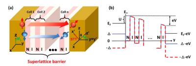
Researchers from the National Taiwan University developed a new ultra low power STT-MRAM architecture, called Super Lattice STT-MRAM, or SL-STT-MRAM. The researchers say that SL-STT-MARM simultaneously achieves ultra-high MR ratio, high-speed switching, and low RA.

SL STT MRAM structure

An SL-STT-MRAM is based on an SL-STT-MTJ, which uses a superlattice barrier to replace the single crystalline (MgO) barrier in traditional STT-MTJ. The superlattice barrier is made of alternating metal and insulator layers, in which only amorphous rather than single crystalline is used in the insulator. The SL-STT-MRAM features higher reliability for repeated writing than compared to traditional MgO based STT-MRAM.

Read the full story Posted: Dec 23,2019

Intel researchers demonstrate 2MB STT-MRAM arrays suitable for on-chip L4 cache applications

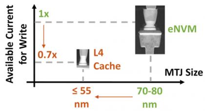
Intel researchers have demonstrated 2MB STT-MRAM devices that are suitable for on-chip L4 cache applications. Intel says these devices feature data retention, endurance and bit error rates good enough for L4 cache.

Intel slide - STT MRAM L4 Cache

Intel's new STT-MRAM features 20 nm write times, 4 ns read times, an endurance of 1012 cycles and memory retention of one second at 110 degrees. The bit rates are good enough to be handled with error-correcting code (ECC) techniques. To achieve these features, Intel reduced the magnetic junction size to 55 nm (from 70-80 nm it had achieved before).

Read the full story Posted: Dec 11,2019

Researchers in Japan developed a high-speed SOT-MRAM memory cell compatible with 300mm Si CMOS technology

Researchers at Tohoku University demonstrated a high-speed spin-orbit-torque MRAM (SOT-MRAM) memory cell compatible with 300 mm Si CMOS technology.

The SOT device achieved high-speed switching (down to 0.35 ns) and a high thermal stability factor (E/kBT 70) which the researchers say is sufficient for high speed non-volatile memory applications. The device can withstand annealing at 400°C. The researchers used these devices to create a complete SOT-MRAM memory cell.

Read the full story Posted: Dec 10,2019