Samsung Foundry to start offering STT-MRAM by 2019

Back in July 2016 (yes, we missed that one, but better late than never), Samsung Foundry's business development chief Kelvin Low said that the company is set to offer STT-MRAM on its 28nm FDSOI manufacturing process by the end of 2018.

To be more precise, the STT-MRAM in 2018 will be on a not-finalized process (what Samsung calls Risk Production Phase) - and real volume production will only begin in 2019. Samsung will be pushing its eFlash 28nm production before STT-MRAM will be available - but the company expects MRAM to be a favorite in the long term.

Read the full story Posted: Sep 23,2016

IBM demonstrated 11nm STT-MRAM junction, says "time for STT-MRAM is now"

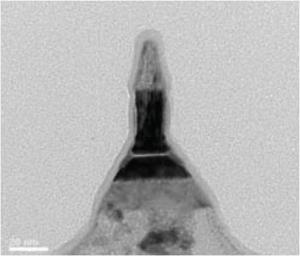
IBM researchers, in collaboration with Samsung researchers, demonstrated switching MRAM cells for devices with diameters ranging from 50 down to 11 nanometers in only 10 nanoseconds, using only 7.5 microamperes. The researchers say that this is a significant achievement on the way to high-density low-power STT-MRAM.

IBM TEM image of a 11-nm junction

Using perpendicular magnetic anisotropy (PMA), the researchers can deliver good STT-MRAM performance down to 7×10⁻¹⁰ write-error-rate with 10 nanosecond pulses using switching currents of only 7.5 microampere.

Read the full story Posted: Jul 08,2016

Samsung will be ready with MRAM chips "soon"

Samsung's semiconductor chief Kim Ki-nam says that Samsung is developing next-generation memory technologies, such as MRAM and RRAM. According to Kim "Samsung will commercialize MRAMs and ReRAMs according to our own schedule. We are on our way and will be ready soon"

Samsung targets MRAM as an update to DRAM memory, while RRAM will be used as a storage memory to replace NAND.

Read the full story Posted: Apr 21,2016

Yole sees STT-MRAM as the most suitable technology to start replacing DRAM in 2018

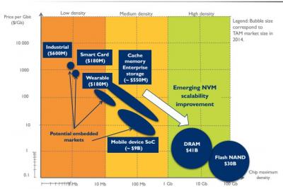
Yole Developpement released a new emerging-memory market report in which they try to asses the future of the memory market. Yose says that Phase-change memory (PCM) is pretty much dead, and the two main emerging memory technologies are MRAM and Resistive random Access Memory (ReRAM or RRAM).

Yole Développement emerging memory market slide (2015)

While RRAM is very promising in the near future, with support from Micron (they plan to release RRAM chips in 2015) and Panasonic while other players are expected to react quickly. RRAM and STT-MRAM will compete in 2015-2016 in some standalone markets (such as embedded MCU, wearables and smart cards and the storage class memory for enterprise storage which will be the biggest market), and it's not clear yet which technology will be the most popular.

Read the full story Posted: Feb 08,2015

Samsung are collaborating with 15 partners on STT-MRAM innovations

Back in June 2013 Samsung Electronics launched a global research outreach program aimed towards STT-MRAM innovation. The Samsung Global MRAM Innovation (SGMI) wanted wanted to reach out to colleges, universities and research labs from all over the world to explore breakthrough and innovative STT-MRAM research.

Samsung ran a short ad campaign on MRAM-Info and Spintronics-Info to help discover partners. Samsung informed us that they received lots of best and most novel proposals on a range of compelling research subjects. They are now collaborating with 15 SGMI partners. Hopefully we'll someday hear of the advances made through these collaborations.

Read the full story Posted: Apr 06,2014

Samsung to looking for global STT-MRAM research partners, offers funding and collaboration

Samsung Electronics launched a new global research outreach program aimed towards STT-MRAM innovation. The Samsung Global MRAM Innovation (SGMI) is looking for colleges, universities and research labs from all over the world to explore breakthrough and innovative STT-MRAM research.

Samsung invites submissions for novel ideas on STT-MRAM research - and the selected proposals will receive financial support from Samsung. Samsung will give around $70,000 to $150,000 for one year research (which may be extended for up to three years). They may also offer larger funds for exceptional proposals. The deadline for submission is September 28, 2013.

Read the full story Posted: Jun 04,2013

Samsung developed a perpendicular MTJ at 17nm

Samsung developed a perpendicular MTJ element using 17nm technology - the world's smallest. This paves the way towards sub-20nm STT-MRAM. Up until now it was believed that to create such a small P-MTJ you will have to use a multi-layer structure and a rare-earth material for the ferromagnetic electrode. Samsung however used regular materials and structure (Ta/CoFeB/MgO/Ta) and optimized the oxidation process for the tunnel insulator (MgO).

By increasing the anisotropic energy on the joint interface the perpendicular magnetization of the ferromagnetic electrode was stabilized. Samsung reports a thermal stability factor of 34, a TMR ratio of 70% and a writing current of 44microampere with a perpendicular magnetization MTJ element whose cross-section area is 17 x 40nm. There is still room for improvement in the thermal stability factor in order to achieve over 1Gbit capacity at 20nm. This can be realized by making more improvements to the newly developed oxidation process for the tunnel insulator

Read the full story Posted: Dec 11,2011

Samsung acquires Grandis

Samsung announced that it has acquired Grandis, developer of STT-MRAM technology. We do not have any financial details yet, but Grandis' CEO Frahad Tabrizi said that this deal serves as a& "very successful exit" for Grandis's investors. Grandis raised $15 million since it was founded in 2002 (and also raised about the same from DARPA grants including a $8.6 million second-phase project granted in June 2010).

Grandis licensed their technology to several companies. We know that Hynix licensed it in 2008. The company was also collaborating with Renesas technologies. Hynix and Grandis were developing a compact in-plane MTJ based STT-RAM device that uses modified DRAM processes at 54nm.

Read the full story Posted: Aug 02,2011

IBM, Samsung and Hynix-Grandis report STT-MRAM research progress

During the International Electron Device Meeting (IEDM) exhibition we got some updates about STT-MRAM research done at IBM, Samsung and Hynix-Grandis (who are researching STT-MRAM together).

IBM is working together with TDK and has presented a new 4-kbit perpendicular STT-MRAM array using tunnel junctions. Samsung has presented an on-axis MRAM with a novel MTJ, which they say open he way towards sub-30nm scaling. Using ferromagnetic electrode and a different MTJ structure design, Samsung think that they can scale this to a sub-20nm level.

Read the full story Posted: Dec 08,2010

Hynix and Samsung to co-develop STT-RAM in a $40 million project

The Korean Government has decided to fund STT-RAM research for Hynix and Samsung in a $40 million project. The government will pay around half of the sum for the project, which is intended to run till 2014. The project calls for the government to work with Samsung and Hynix together for research and development on STT-MRAM chips. Korea aims to control around 45% of the 30-nano type memory chip market by 2015.

The companies have already opened a new laboratory at Hangyang University's fusion technology center. It is already equipped with a fully operational 300mm magnetic thin film deposition system and other chip-making facilities.

Read the full story Posted: Nov 26,2009