Embedded MRAM

Tiempro Secure's Secure Element succesfully implemented in GlobalFroundries 22-nm process with MRAM memory

France-based Tiempro Secure announced that its TESIC RISC-V Secure Element was implemented in GlobalFoundries’ 22-nm platform with embedded MRAM, after a rigorous characterization process.

Tiempo Secure says it leveraged its long-standing know-how in Secure IP, to adapt its TESIC  design to the 22FDX technology process node. The TESIC platform has a secure architecture based on a RISC-V CPU core, several memory types (including ROM, RAM, Cache,  Crypto-RAM, and MRAM), random number generators, security  sensors, and secure crypto-accelerators. This provides a pre-silicon  certified IP solution on GF’s 22FDX to SoC manufacturers who require a high-end Secure  Element.

Read the full story Posted: Mar 21,2024

NXP and TSMC to offer 16 nm FinFET automotive embedded MRAM

NXP Semiconductors announced a collaboration with TSMC to offer automotive embedded MRAM, in TSMC's 16 nm FinFET technology. NXP says that as automakers transition to software-defined vehicles, they need to support multiple generations of software upgrades on a single hardware platform. Bringing together NXP’s high-performance S32 automotive processors with fast and highly reliable next-generation MRAM in 16 nm FinFET technology provides the ideal hardware platform for this transition.

The new MRAM memory will be able to udpate 20MB of code in ~3 seconds compared to flash memories that take about 1 minute, which will minimize the downtime associated with software updates. MRAM also provides a highly reliable technology for automotive mission profiles by offering up to one million update cycles, a level of endurance 10x greater than flash and other emerging memory technologies.

Read the full story Posted: May 16,2023

Samsung researchers update on the company's 14 nm eMRAM project

Researchers from Samsung will soon present at IEDM 2022 a new research paper that will discuss the company's latest achievements in scaling down its MRAM technology to the company's 14nm FinFET logic process.

Samsung eMRAM image

The Samsung researchers produced a stand-alone memory with a write energy requirement of 25 pJ per bit and active power requirements of 14 mW for reading and 27 mW for writing at a 54Mbyte per second data rate. The cycling  is 10^14 cycles and when scaled to a 16Mbit device, a chip would occupy 30 square millimeters.

Read the full story Posted: Oct 26,2022

Renesas develops 22-nm circuit technologies for embedded STT-MRAM

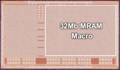
Renesas announced that it has developed 22-nm embedded STT-MRAM circuit technologies. Renesas developed a test 32-megabit (Mbit) chip with an embedded MRAM memory cell array that achieves 5.9-nanosecond (ns) random read access at a maximum junction temperature of 150°C, and a write throughput of 5.8-megabyte-per-second (MB/s).

To achieve this performance, Renesas developed two technologies. The first is a fast read technology employing high-precision sense amplifier circuit, utilizing capacitive coupling. The second is a fast write technology, with simultaneous write bit number optimization and shortened mode transition time.

Read the full story Posted: Jun 18,2022

Samsung is progressing towards 14 nm eMRAM

In March 2019 Samsung Electronics announced that it has started to mass produce its first embedded MRAM devices, made using the company's 28nm FD-SOI process. In early 2021 Samsung announced that it managed to improve the MTJ function of its MRAM, which makes it suitable for more applications, and today, at the company's 5th Annual Samsung Foundry Forum, Samsung provides more details on its MRAM roadmap.

Samsung eMRAM image

Samsung says it is advancing its 14 nm process which will support flash-type embedded MRAM which enables increased write speed and density. Samsung targets applications such as micro controller units (MCUs), IoT and wearables for its next-gen eMRAM.

Read the full story Posted: Oct 08,2021

Embedded-MRAM, what the future holds

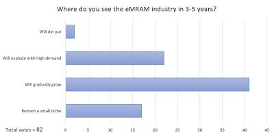
Embedded MRAM solutions are now entering the market, as leading foundries Samsung, TSMC and GlobalFoundries are scaling-up and ramping up their solutions.

Embedded MRAM market, MRAM-Info poll results 2021-09

This has been a slow process, as getting next-generation technologies into large fab is never an easy task, but we are finally seeing these foundries start to offer these technologies to their customers.

Read the full story Posted: Sep 20,2021

Researchers suggest using stochastic MRAM elements to create highly efficient AI neural network devices

Researchers from Northwestern University developed a new method of building artificial neural networks using MRAM-based stochastic computing units. The researchers say that this design could enable AI devices that are highly energy efficient.

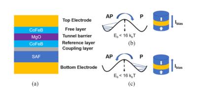
MTJ-based stochastic computing unit structure (Northwestern University)

Embedded MRAM technologies are being adopted at major foundries, which enable the use of these technologies for unconventional computing architectures that use the stochasticity of MRAM cells (rather than their nonvolatility), to perform energy-efficient computing operations. MRAM cells exhibit stochastic switching characteristics, which is a challenge for reliable memory devices. But for neural networks, this can be taken advantage of if the MTJs are appropriately designed.

Read the full story Posted: Jul 07,2021

TSMC shows its eMRAM technology roadmap

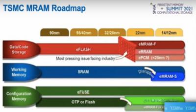
During a presentation during Persistent Memory Summit, a new slide from TSMC was shown that describes the company's eMRAM roadmap:

TSMC memory roadmap (Persistant Mmemory Summit 2021)

As we already know, TSMC is offering 22nm eMRAM option as an eFlash alternative. The company is also looking to develop 14/12 nm eMRAM option to replace SRAM memory (this is interesting as before it was revealed that the company is developing 16nm MRAM). Finally eMRAM is touted as a possible replacement for configuration memory (eFUSE / OTP / Flash).

Read the full story Posted: May 06,2021

Everspin reported its preliminary Q4 2020 and full-year 2020 financial results

Everspin Technologies announced its preliminary Q4 2020 financial results. Total revenues were $10 million, down from $10.1 million in Q3 and up from $9.7 million in Q4 2019. Net loss int he quarter was $1.6 million, but the company generated $0.6 million in cash flow - Everspin's second consecutive positive cash flow from operations quarter.

Everspin Technologies chip photo

Looking at FY2020, Everspin's revenues increased 12.1% to $42 million. At the end of the year, Everspin had $14.6 million in cash and equivalents. In Q4 2020, the company also received its first royalty revenue from GF for embedded 22FDX process MRAM.

Read the full story Posted: Mar 01,2021

Samsung improves its MRAM performance, will expand its target applications

In March 2019 Samsung Electronics announced that it has started to mass produce its first embedded MRAM, made using the company's 28nm FD-SOI process. The company now announced that it managed to improve the MTJ function of its MRAM, which makes it suitable for more applications.

Samsung eMRAM image

Samsung will now expand the application of its eMRAM solutions to more markets - specifically the automotive, wearable, graphic memory, low level cache, internet of things and edge artificial intelligence markets.

Read the full story Posted: Feb 05,2021