December 2019

New USMR MRAM structure promises extremly simple design

Researchers from Tokyo's Institute of Technology (Tokyo Tech) developed a new MRAM cell structure (called USMR MRAM) that features a very simple structure with only two layers - which could hopefully enable lower-cost MRAM devices.
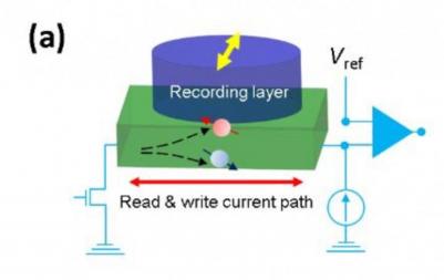
USMR MRAM cell structure image

The new design uses a combination of a topological insulator with a ferromagnetic semiconductor which enables a giant unidirectional spin Hall magnetoresistance (USMR).
Read the full story Posted: Dec 29,2019

New super-lattice SL-STT-MRAM enable faster and more efficient memory architecture

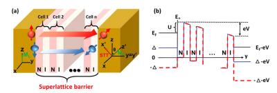
Researchers from the National Taiwan University developed a new ultra low power STT-MRAM architecture, called Super Lattice STT-MRAM, or SL-STT-MRAM. The researchers say that SL-STT-MARM simultaneously achieves ultra-high MR ratio, high-speed switching, and low RA.

SL STT MRAM structure

An SL-STT-MRAM is based on an SL-STT-MTJ, which uses a superlattice barrier to replace the single crystalline (MgO) barrier in traditional STT-MTJ. The superlattice barrier is made of alternating metal and insulator layers, in which only amorphous rather than single crystalline is used in the insulator. The SL-STT-MRAM features higher reliability for repeated writing than compared to traditional MgO based STT-MRAM.

Read the full story Posted: Dec 23,2019

Mentor to provide IC test solutions for Arm's eMRAM compiler IP

Mentor announced that it will provide a unique IC test solution for the Arm's eMRAM compiler IP which is built on Samsung Foundry’s 28nm FDSOI process technology.

Mentor says it is working with Arm to leverage industry-leading Tessent software Built-In Self-Test (BIST) Design-for-Testability (DFT) technologies for testing the next-generation of Arm's eMRAM compiler IP in development.

Read the full story Posted: Dec 18,2019

Intel researchers demonstrate 2MB STT-MRAM arrays suitable for on-chip L4 cache applications

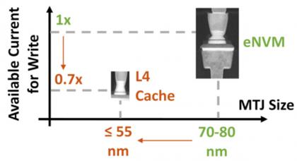
Intel researchers have demonstrated 2MB STT-MRAM devices that are suitable for on-chip L4 cache applications. Intel says these devices feature data retention, endurance and bit error rates good enough for L4 cache.

Intel slide - STT MRAM L4 Cache

Intel's new STT-MRAM features 20 nm write times, 4 ns read times, an endurance of 1012 cycles and memory retention of one second at 110 degrees. The bit rates are good enough to be handled with error-correcting code (ECC) techniques. To achieve these features, Intel reduced the magnetic junction size to 55 nm (from 70-80 nm it had achieved before).

Read the full story Posted: Dec 11,2019

Researchers in Japan developed a high-speed SOT-MRAM memory cell compatible with 300mm Si CMOS technology

Researchers at Tohoku University demonstrated a high-speed spin-orbit-torque MRAM (SOT-MRAM) memory cell compatible with 300 mm Si CMOS technology.

The SOT device achieved high-speed switching (down to 0.35 ns) and a high thermal stability factor (E/kBT 70) which the researchers say is sufficient for high speed non-volatile memory applications. The device can withstand annealing at 400°C. The researchers used these devices to create a complete SOT-MRAM memory cell.

Read the full story Posted: Dec 10,2019

Researchers demonstrate a new memory device using an OLED and a MOS capacitor

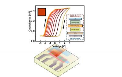
Researchers from TU Dresden developed a novel memory device that is based on a combination of an light emitting material and a metal-oxide semiconductor (MOS) capacitor.

pinMOS memory structure (TU Dresden)

The so-called pinMOS device is a non-volatile memory-capacitor with high repeatability and reproducibility. pinMOS devices can store several states, since charges can be added or removed in controllable amounts. This device can also be controlled (read and write) both electrically and optically. The light emitting material is an OLED device.

Read the full story Posted: Dec 01,2019