The best of 2016 - top MRAM stories
2016 is soon over - and this was a very exciting year for the MRAM industry. Everspin floated on the Nasdaq and started sampling 256Mb STT-MRAM chips, other companies also announced and launched MRAM devices, and IBM announced that the "time for STT-MRAM is now". Interest in MRAM technologies is certainly on the rise!
Here are the top 10 stories posted on MRAM-Info in 2016, ranked by popularity (i.e. how many people read the story):
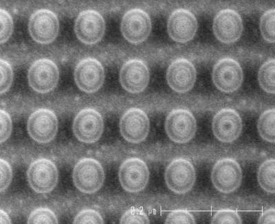
- IBM demonstrated 11nm STT-MRAM junction, says "time for STT-MRAM is now" (Jul 8)
- Everspin starts sampling 256Mb ST-MRAM chips, plans 1Gb chips by the end of 2016 (Apr 15)
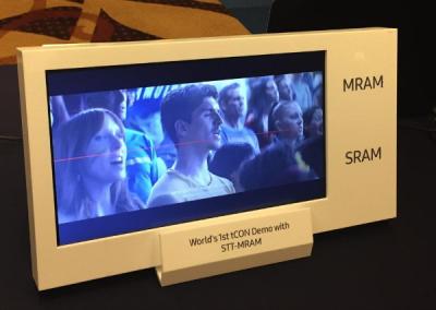
- Samsung will be ready with MRAM chips "soon" (Apr 21)
- Researchers suggest and demonstrate a new scheme of spin-orbit-torque (SOT) induced magnetization switching (Mar 22)
- IBM demonstrates Everspin's ST-MRAM in its ConTutto platform in a Power8 system (Apr 9)
- New etching process developed specifically for MRAM production (Mar 6)
- Everspin starts shipping perpendicular-MTJ based ST-MRAM chip samples (Aug 9)
- Researchers developed a spin-orbit torque based device, an alternative to STT (Jul 22)
- New logo and updated design (Jan 8)
- Spin Transfer Technologies produced working 60-nm STT-MRAM prototypes (Feb 4)

