July 2016

Yole Developpement sees MRAM, RRAM and PCM memories generating $4.6 billion in 2021

Yole Developpement says that the emerging Non-Volatile Memory (NVM) market is still small, generating only $53 million in sales in 2015. The market is still limited to niche markets due to the limited densities.

Next-gen memory, time to market (Yole, 2015)

Yole sees the market growing very quickly, though, to reach $4.6 billion by 2021 - a CAGR of 110%. Yole says that the clear go-to market for emerging-NVM will be storage-class memory. High-capacity SCM applications will use either phase-change memory or RRAM memory, while applications that require high endurance and speed will adopt STT-MRAM memories.

 
Read the full story Posted: Jul 28,2016

Researchers developed a spin-orbit torque based device, an alternative to STT

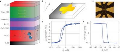
Researchers from the Trinity College in Dublin developed a new device using a stack of five metal layers (including a platinum layer and an iron-based layer) that can be used to control the spin of electrons - using "spin–orbit torque", or SOT, an alternative to spin-transfer torque (STT) - but without an external field.

SOT switching without an eternal field (TCD)

The basic idea is that when a current is run through the platinum, the electrons split into two groups by their spin (that's the SOT effect). Electrons are inserted into the iron-based "storage layer" and the spin of those electrons can be changed. The rest of the layers act like a thin-film magnet which helps determine the spin of the electrons.

Read the full story Posted: Jul 22,2016

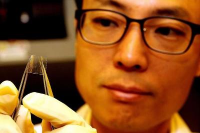
NUS researchers developed the world's first bendable MRAM device

Researchers from the National University of Singapore (NUS) developed what they say is the world's first flexible (bendable, actually) MRAM device. Flexible OLED displays are already entering the market, and now researchers are developing other flexible components, which will be needed if truly bendable and flexible devices are to be possible.

Flexible MRAM device, NUS 2016

The researchers used a new fabrication method, that enabled them to deposit the magnetic memory on a plastic substrate, and not a silicon one. This was achieved following a two-year collaboration with Yonsei University, Ghent University and Singapore's Institute of Materials Research and Engineering.

Read the full story Posted: Jul 20,2016

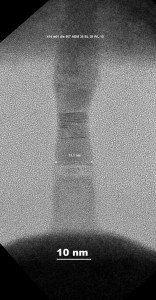
IBM demonstrated 11nm STT-MRAM junction, says "time for STT-MRAM is now"

IBM researchers, in collaboration with Samsung researchers, demonstrated switching MRAM cells for devices with diameters ranging from 50 down to 11 nanometers in only 10 nanoseconds, using only 7.5 microamperes. The researchers say that this is a significant achievement on the way to high-density low-power STT-MRAM.

IBM TEM image of a 11-nm junction

Using perpendicular magnetic anisotropy (PMA), the researchers can deliver good STT-MRAM performance down to 7×10⁻¹⁰ write-error-rate with 10 nanosecond pulses using switching currents of only 7.5 microampere.

Read the full story Posted: Jul 08,2016