STT-MRAM (also called STT-RAM or sometimes ST-MRAM and ST-RAM) is an advanced type of MRAM devices. STT-MRAM enables higher densities, low power consumption and reduced cost compared to regular (so-called Toggle MRAM) devices. The main advantage of STT-MRAM over Toggle MRAM is the ability to scale the STT-MRAM chips to achieve higher densities at a lower cost.
STT-MRAM has the potential to become a leading storage technology as it is a high-performance memory (can challenge DRAM and SRAM) that can scale well below 10nm and challenge the low cost of flash memory.
What is STT-MRAM?
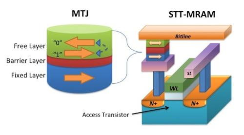
STT stands for Spin-Transfer Torque. In an STT-MRAM device, the spin of the electrons is flipped using a spin-polarized current. This effect is achieved in a magnetic tunnel junction (MTJ) or a spin-valve, and STT-MRAM devices use STT tunnel junctions (STT-MTJ). A spin-polarized current is created by passing a current though a thin magnetic layer. This current is then directed into a thinner magnetic layer which transfers the angular momentum to the thin layer which changes its spin.
What is perpendicular STT-MRAM?
A "regular" STT-MRAM structure (similar to the one you see above) uses an in-plane MTJ (iMTJ). Some STT-MRAM devices use a more optimized structure called perpendicular MTJ (pMTJ) in which the magnetic moments are perpendicular to the silicon substrate surface.
Perpendicular STT-MRAM is more scalable compared to iMTJ STT-MRAM and is also more cost competitive. Perpendicular STT-MRAM is thus a more promising technology to replace DRAM and other memory technologies
STT-MRAM chips
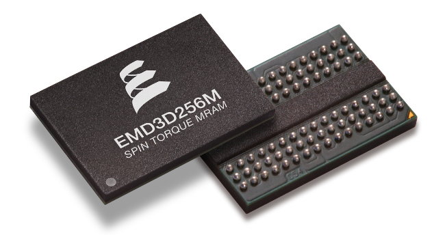
Several companies, including IBM and Samsung, Everspin, Avalanche Technologies, Spin Transfer Technologies and Crocus are developing STT-MRAM chips. In April 2016 Everspin announced that it started shipping 256Mb ST-MRAM samples to customers. The new chips demonstrate interface speeds comparable to DRAM, with DDR3 and DDR4 interfaces. Volume production is expected "soon".
In August 2016 Everspin started sampling pMTJ-based ST-MRAM chips. The first chips are also 256Mb in size, but the pMTJ versions offer improved performance, higher endurance, lower power, and better scalability compared to previous iMTJ ST-MRAM products. Everspin is now ramping out 256Mb pMTJ ST-MRAM production and is developing a scaled-down 1Gb version.
Latest STT-MRAM news