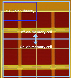
Researchers from Japan's Tohoku University developed a technology to stack magnetic tunnel junctions (MTJs) directly on the the vertical interconnect access (via) without causing deterioration to its electric/magnetic characteristics. The researchers say that this technique can reduce the chip area of STT-MRAM.

The via in an integrated circuit design is a small opening that allows a conductive connection between the different layers of a semiconductor device. Placing the MTJ directly on the via holes has been avoided because it can degrade the MTJ's characteristics because the MTJ is very sensitive to the quality of the surface of its lower electrode.
The new technology is actually a polishing process that prevents any interference between the MTJ and its lower electrode. The researchers fabricated a test 2-Mbit STT-MRAM that uses the new technology. The test chip showed a 70% improvement in its memory bit yield compared to standard STT-MRAM, and its memory cell area is reduced by 30%.